LPC5411x All information provided in this document is subject to legal disclaimers. © NXP Semiconductors N.V. 2018. All rights reserved.
Product data sheet Rev. 2.1 — 9 May 2018 46 of 105
NXP Semiconductors
LPC5411x
32-bit ARM Cortex-M4/M0+ microcontroller
8. Limiting values
[1] The following applies to the limiting values:
a) This product includes circuitry specifically designed for the protection of its internal devices from the damaging effects of excessive
static charge. Nonetheless, it is suggested that conventional precautions be taken to avoid applying greater than the rated
maximum.
b) Parameters are valid over operating temperature range unless otherwise specified. All voltages are with respect to V
SS
unless
otherwise noted.
c) The limiting values are stress ratings only and operating the part at these values is not recommended and proper operation is not
guaranteed. The conditions for functional operation are specified in Table 20
.
[2] Maximum/minimum voltage above the maximum operating voltage (see Table 20
) and below ground that can be applied for a short time
(< 10 ms) to a device without leading to irrecoverable failure. Failure includes the loss of reliability and shorter lifetime of the device.
[3] The peak current is limited to 25 times the corresponding maximum current.
[4] Human body model: equivalent to discharging a 100 pF capacitor through a 1.5 k series resistor.
[5] V
DD
present or not present. Compliant with the I
2
C-bus standard. 5.5 V can be applied to this pin when V
DD
is powered down.
[6] Applies to all 5 V tolerant I/O pins except true open-drain pins.
[7] Including the voltage on outputs in 3-state mode.
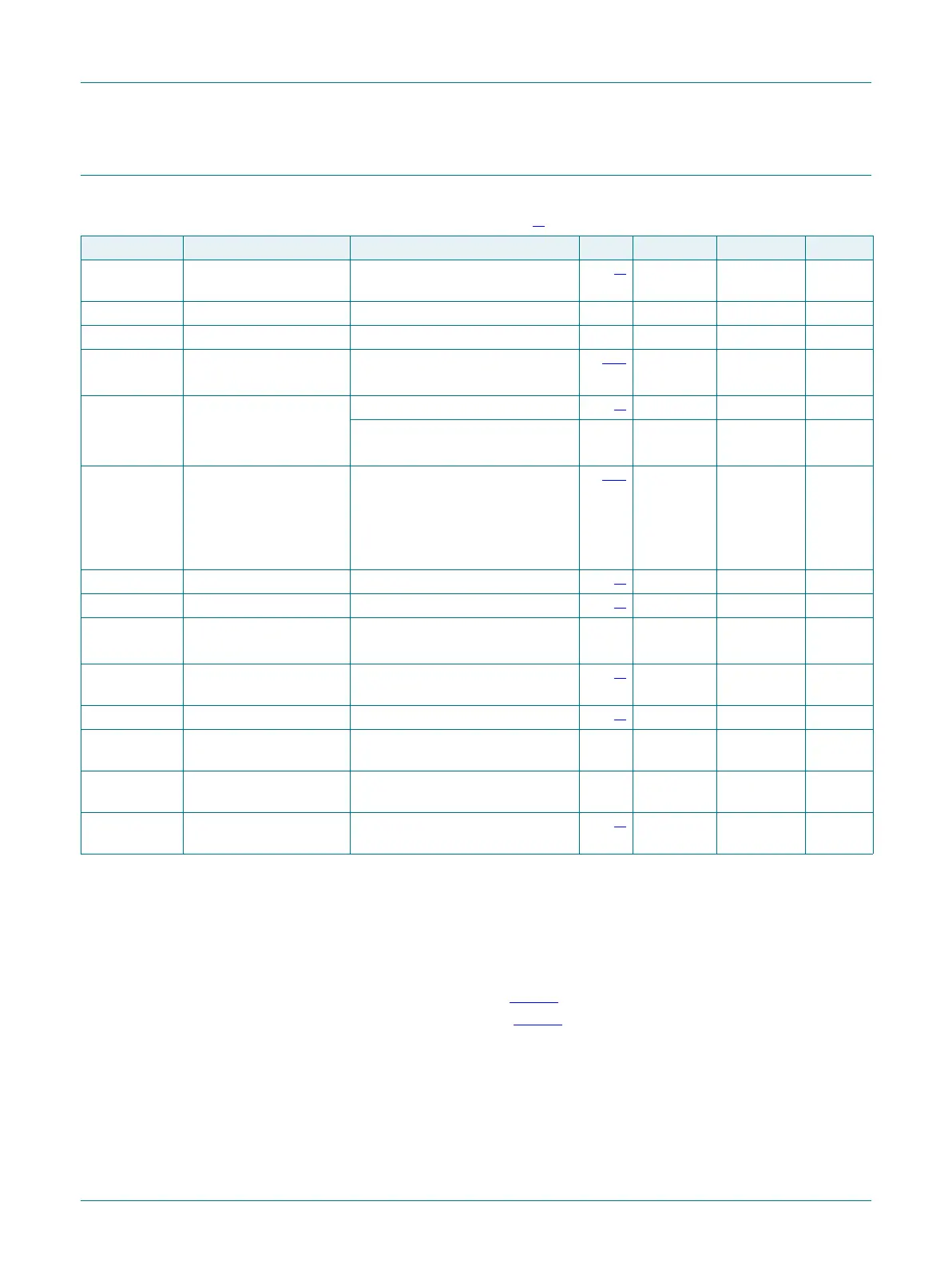
Table 10. Limiting values
In accordance with the Absolute Maximum Rating System (IEC 60134).
[1]
Symbol Parameter Conditions Min Max Unit
V
DD
supply voltage (core and
external rail)
on pin V
DD
[2]
0.5 +4.6 V
V
DDA
analog supply voltage on pin V
DDA
0.5 +4.6 V
V
ref
reference voltage on pin VREFP - 0.5 +4.6 V
V
I
input voltage only valid when the V
DD
> 1.8 V;
5 V tolerant I/O pins
[6][7]
0.5 +5.0 V
V
I
input voltage on I2C open-drain pins
[5]
0.5 +5.0 V
USB_DM,
USB_DP pins
0.5 +5.0 V
V
IA
analog input voltage on digital pins configured for an
analog function
[8][9]
0.5 V
DD
V
I
DD
total supply current per supply pin
[3]
-60mA
I
SS
total ground current per ground pin
[3]
-60mA
I
latch
I/O latch-up current (0.5V
DD
) < V
I
< (1.5V
DD
);
T
j
< 125 C
-100mA
V
i(rtcx)
32.768 kHz oscillator
input voltage
[2]
0.5 +4.6 V
T
stg
storage temperature
[9]
65 +150 C
T
j(max)
maximum junction
temperature
-+150C
P
tot(pack)
total power dissipation
(per package)
based on package heat transfer,
not device power consumption
-1.5W
V
ESD
electrostatic discharge
voltage
human body model; all pins
[3]
4000 V

 Loading...


