LPC5411x All information provided in this document is subject to legal disclaimers. © NXP Semiconductors N.V. 2018. All rights reserved.
Product data sheet Rev. 2.1 — 9 May 2018 77 of 105
NXP Semiconductors
LPC5411x
32-bit ARM Cortex-M4/M0+ microcontroller
11.13 DMIC subsystem
[1] Based on simulated values and for 2.7 V to 3.6 V.
11.14 USB interface characteristics
Table 34. Dynamic characteristics
T
amb
=
40
C to 105
C; V
DD
= 1.62 V to 3.6 V; C
L
= 30 pF balanced loading on all pins; Input slew = 1 ns, SLEW set to
standard mode for all pins; Bypass bit = 0; Parameters sampled at the 90 % and 10 % level of the rising or falling edge.
Symbol Parameter Conditions Min Typ
[1]
Max Unit
t
DS
data set-up time CCLK = 1 MHz to 12 MHz - 23 - ns
CCLK = 48 MHz to 60 MHz - 13 - ns
CCLK = 96 MHz - 9 - ns
t
DH
data hold time CCLK = 1 MHz to 12 MHz - 0 - ns
CCLK = 48 MHz to 60 MHz - 0 - ns
CCLK = 96 MHz - 0 - ns
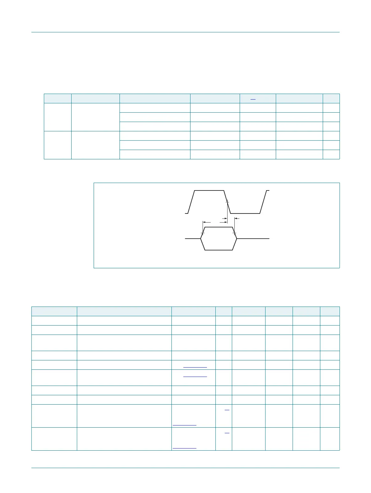
Fig 25. DMIC timing diagram
aaa-017025
CLOCK
DATA
t
SU
t
DH
Table 35. Dynamic characteristics: USB pins (Full-Speed)
C
L
= 50 pF; R
pu
= 1.5 k
on D+ to V
DD
, unless otherwise specified; 3.0 V
V
DD
3.6 V.
Symbol Parameter Conditions Min Typ Max Unit
t
r
rise time 10 % to 90 % 4.0 - 20 ns
t
f
fall time 10 % to 90 % 4.0 - 20 ns
t
FRFM
differential rise and fall time match-
ing
t
r
/t
f
90 - 111.11 %
V
CRS
output signal crossover voltage 1.3 - 2.0 V
t
FEOPT
source SE0 interval of EOP see Figure 26 160 - 175 ns
t
FDEOP
source jitter for differential transition
to SE0 transition
see Figure 26 2-+5ns
t
JR1
receiver jitter to next transition 18.5 - +18.5 ns
t
JR2
receiver jitter for paired transitions 10 % to 90 % 9-+9ns
t
EOPR1
EOP width at receiver must reject as
EOP; see
Figure 26
[1]
40 - ns
t
EOPR2
EOP width at receiver must accept as
EOP; see
Figure 26
[1]
82 --ns

 Loading...


