LPC5411x All information provided in this document is subject to legal disclaimers. © NXP Semiconductors N.V. 2018. All rights reserved.
Product data sheet Rev. 2.1 — 9 May 2018 63 of 105
NXP Semiconductors
LPC5411x
32-bit ARM Cortex-M4/M0+ microcontroller
11. Dynamic characteristics
11.1 Flash memory
[1] Typical ratings are not guaranteed.
[2] Number of erase/program cycles.
[3] Programming times are given for writing 256 bytes from RAM to the flash.
11.2 I/O pins
[1] Simulated data.
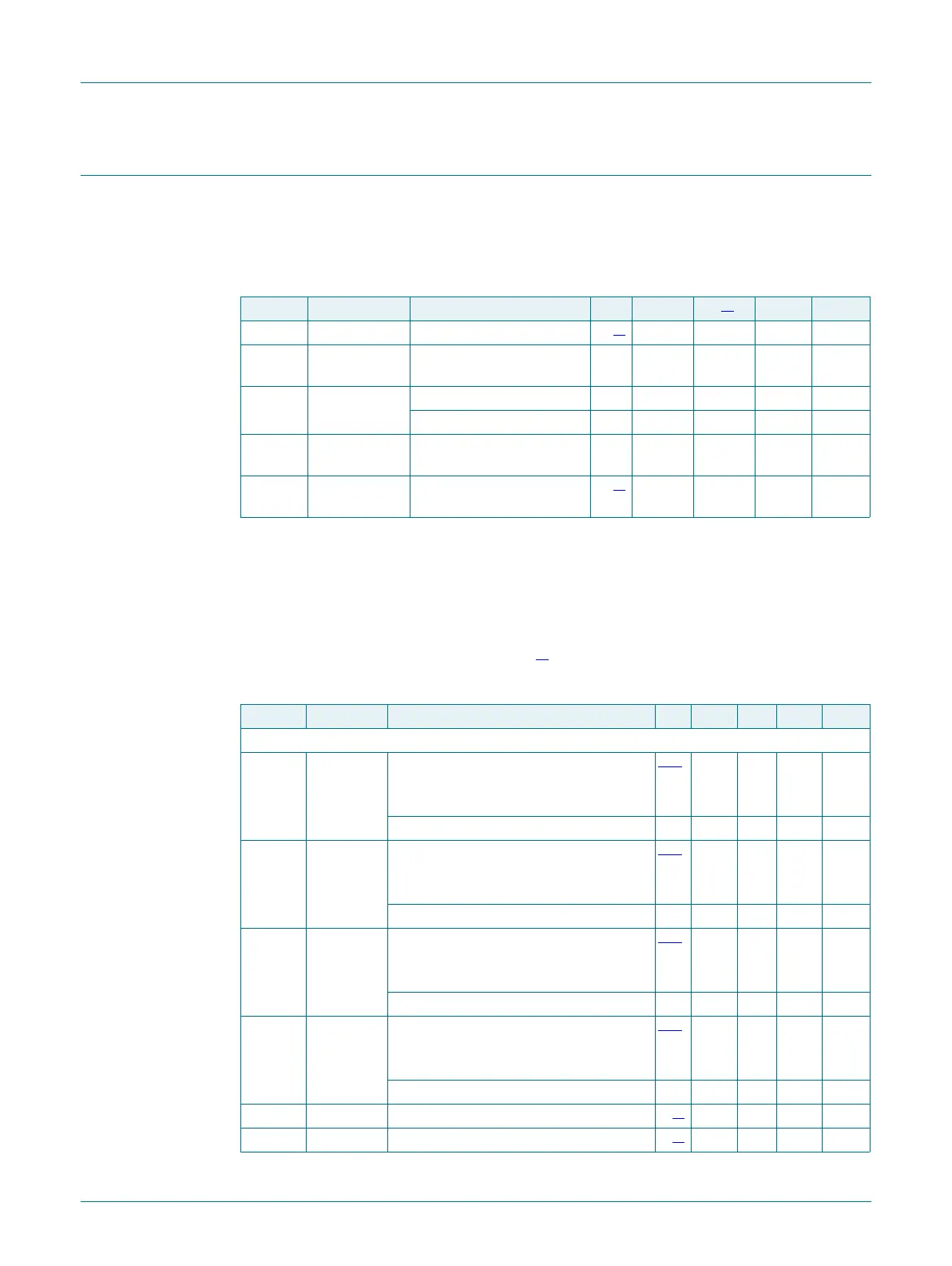
Table 21. Flash characteristics
T
amb
=
40
C to +105
C, unless otherwise specified. 1.62 V
V
DD
3.6 V unless otherwise
specified.
Symbol Parameter Conditions Min Typ
[1]
Max Unit
N
endu
endurance sector erase/program
[2]
10000 - - cycles
page erase/program; page
in a sector
1000 - - cycles
t
ret
retention time powered 10 - - years
unpowered 10 - - years
t
er
erase time page, sector, or multiple
consecutive sectors
-100-ms
t
prog
programming
time
[3]
-1-ms
Table 22. Dynamic characteristic: I/O pins
[1]
T
amb
=
40
C to +85
C unless otherwise specified; 1.62 V
V
DD
3.6 V unless otherwise
specified.
Symbol Parameter Conditions Min Typ Max Unit
Standard I/O pins - normal drive strength
t
r
rise time pin configured as output; SLEW = 1 (fast
mode);
2.7 V V
DD
3.6 V
[2][3]
1.0 - 2.5 ns
1.62 V V
DD
1.98 V 1.6 - 3.8 ns
t
f
fall time pin configured as output; SLEW = 1 (fast
mode);
2.7 V V
DD
3.6 V
[2][3]
0.9 - 2.5 ns
1.62 V V
DD
1.98 V 1.7 - 4.1 ns
t
r
rise time pin configured as output; SLEW = 0
(standard mode);
2.7 V V
DD
3.6 V
[2][3]
1.9 - 4.3 ns
1.62 V V
DD
1.98 V 2.9 - 7.8 ns
t
f
fall time pin configured as output; SLEW = 0
(standard mode);
2.7 V V
DD
3.6 V
[2][3]
1.9 - 4.0 ns
1.62 V V
DD
1.98 V 2.7 - 6.7 ns
t
r
rise time pin configured as input
[4]
0.3 - 1.3 ns
t
f
fall time pin configured as input
[4]
0.2 - 1.2 ns

 Loading...


