LPC5411x All information provided in this document is subject to legal disclaimers. © NXP Semiconductors N.V. 2018. All rights reserved.
Product data sheet Rev. 2.1 — 9 May 2018 80 of 105
NXP Semiconductors
LPC5411x
32-bit ARM Cortex-M4/M0+ microcontroller
12.2 12-bit ADC characteristics
[1] Based on characterization; not tested in production.
[2] Typical ratings are not guaranteed. The values listed are at room temperature (25 C), nominal supply
voltages.
[3] The input resistance of ADC channels 6 to 11 is higher than ADC channels 0 to 5.
[4] C
ia
represents the external capacitance on the analog input channel for sampling speeds of
5.0 Msamples/s. No parasitic capacitances included.
[5] The differential linearity error (E
D
) is the difference between the actual step width and the ideal step width.
See Figure 27
.
[6] The integral non-linearity (E
L(adj)
) is the peak difference between the center of the steps of the actual and
the ideal transfer curve after appropriate adjustment of gain and offset errors. See Figure 27
.
[7] The offset error (E
O
) is the absolute difference between the straight line which fits the actual curve and the
straight line which fits the ideal curve. See Figure 27
.
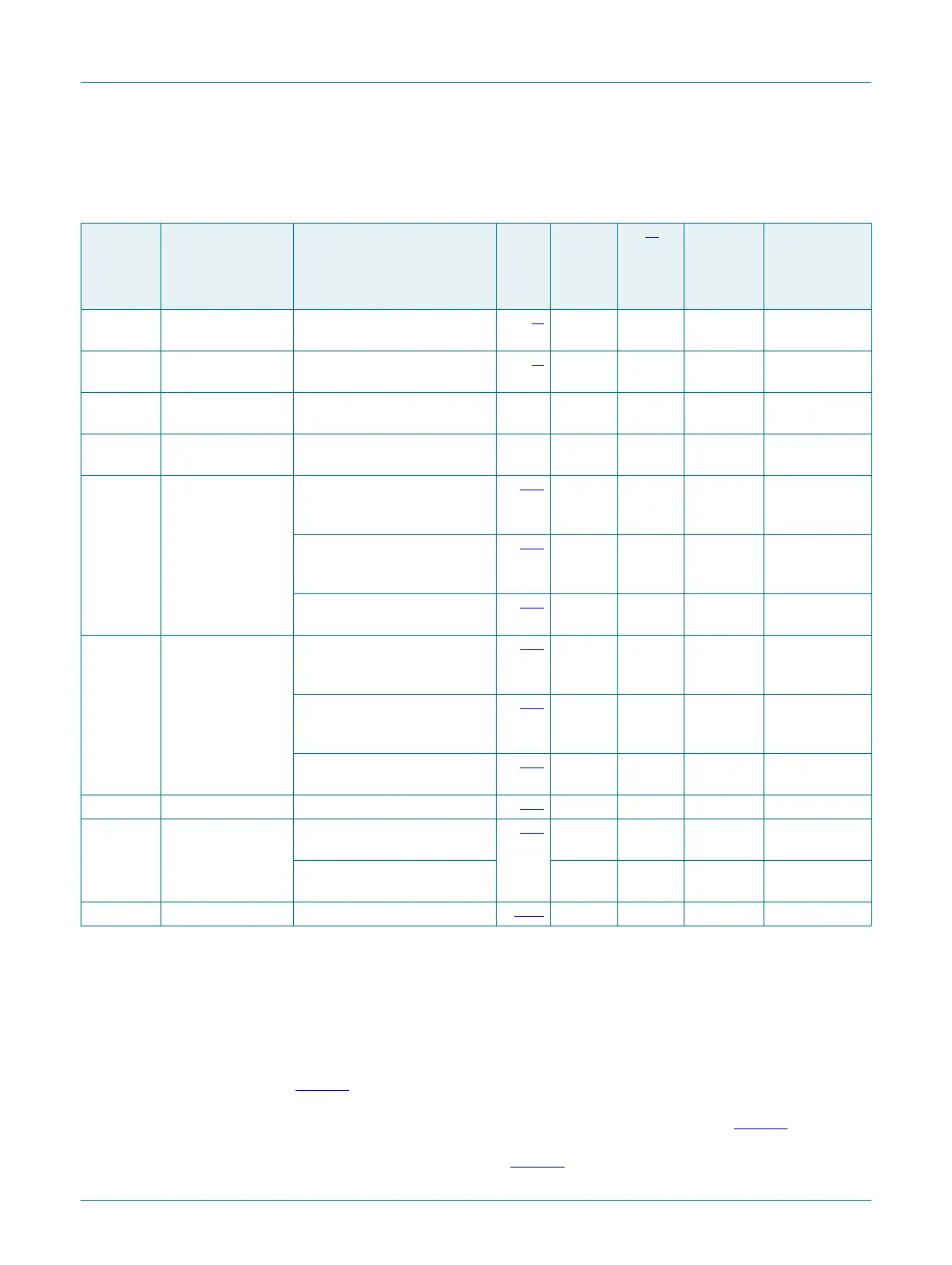
Table 37. 12-bit ADC static characteristics
T
amb
=
40
C to +105
C; 1.62 V
V
DD
3.6 V; V
SSA
= VREFN = GND. ADC calibrated at T
amb
= 25
C.
Symbol Parameter Conditions Min Typ
[2]
Max Unit
V
IA
analog input
voltage
[3]
0- V
DDA
V
C
ia
analog input
capacitance
[4]
-5- pF
f
clk(ADC)
ADC clock
frequency
-80 MHz
f
s
sampling
frequency
- - 5.0 Msamples/s
E
D
differential linearity
error
1.62 V V
DDA
3.6 V
1.62 V VREFP 3.6 V
f
clk(ADC)
= 72 MHz
[1][5]
- 3.0 - LSB
2.0 V V
DDA
3.6 V
2.0 V VREFP 3.6 V
f
clk(ADC)
= 80 MHz
[1][5]
- 3.0 - LSB
V
DDA
= VREFP = 1.62 V
f
clk(ADC)
= 80 MHz
[1][5]
- 7.1 - LSB
E
L(adj)
integral
non-linearity
1.62 V V
DDA
3.6 V
1.62 V VREFP 3.6 V
f
clk(ADC)
72 MHz
[1][6]
- 5.0 - LSB
2.0 V V
DDA
3.6 V
2.0 V VREFP 3.6 V
f
clk(ADC)
= 80 MHz
[1][6]
- 4.0 - LSB
V
DDA
= VREFP = 1.62 V
f
clk(ADC)
= 80 MHz
[1][6]
- 9.0 - LSB
E
O
offset error calibration enabled
[1][7]
- 1.2 - mV
V
err(FS)
full-scale error
voltage
1.62 V V
DDA
2.0 V
1.62 V VREFP 2.0 V
[1][8]
- 3.5 LSB
2.0 V V
DDA
3.6 V
2.0 V VREFP 3.6 V
- 2.0 LSB
Z
i
input impedance f
s
= 5.0 Msamples/s
[9][10]
17.0 - - k

 Loading...


