LPC5411x All information provided in this document is subject to legal disclaimers. © NXP Semiconductors N.V. 2018. All rights reserved.
Product data sheet Rev. 2.1 — 9 May 2018 81 of 105
NXP Semiconductors
LPC5411x
32-bit ARM Cortex-M4/M0+ microcontroller
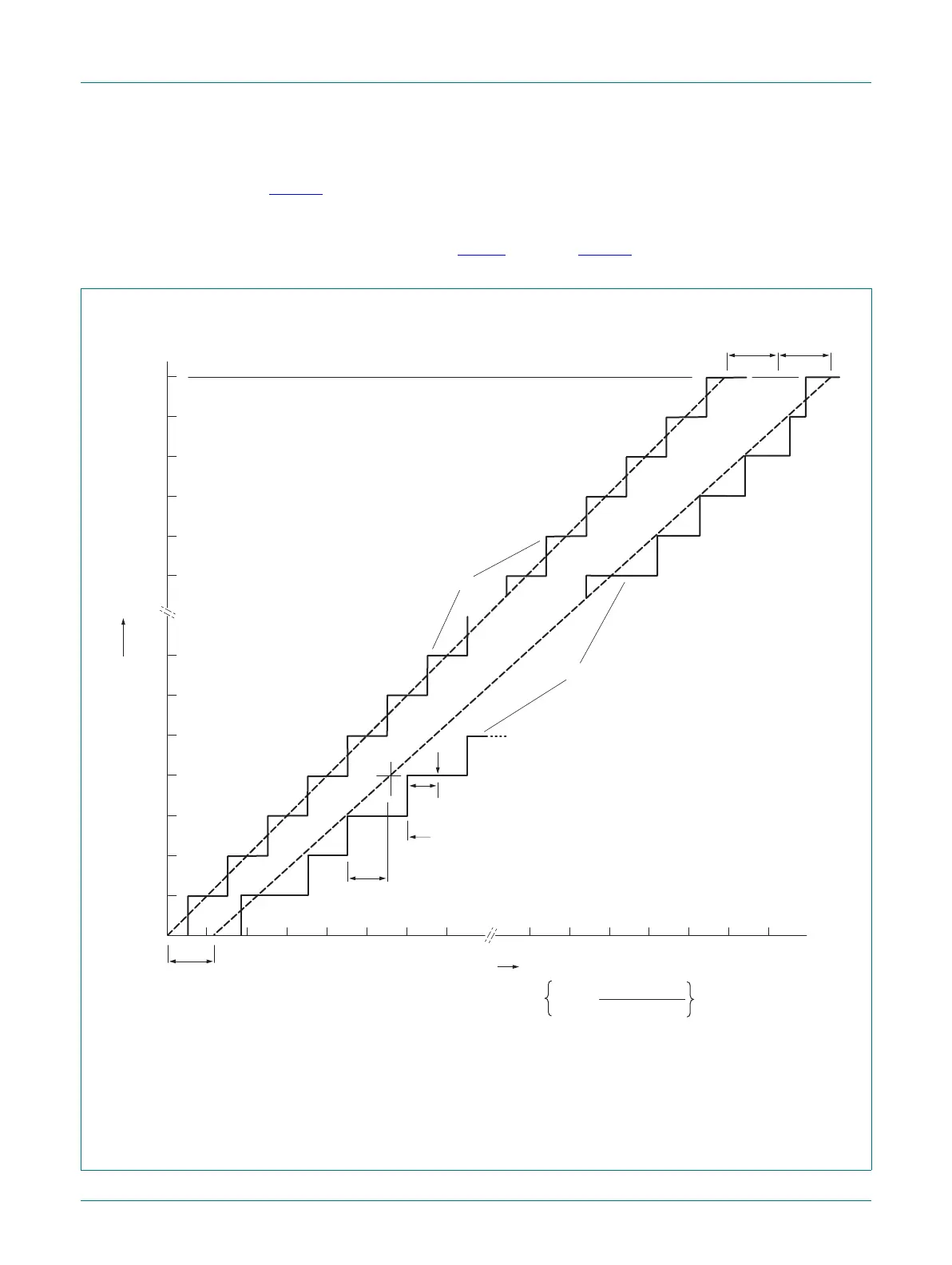
[8] The full-scale error voltage or gain error (E
G
) is the difference between the straight-line fitting the actual
transfer curve after removing offset error, and the straight line which fits the ideal transfer curve. See
Figure 27
.
[9] T
amb
= 25 C; maximum sampling frequency f
s
= 5.0 Msamples/s and analog input capacitance C
ia
=5pF.
[10] Input impedance Z
i
is inversely proportional to the sampling frequency and the total input capacity including
C
ia
and C
io
: Z
i
1 / (f
s
C
i
). See Table 20 for C
io
. See Figure 28.
(1) Example of an actual transfer curve.
(2) The ideal transfer curve.
(3) Differential linearity error (E
D
).
(4) Integral non-linearity (E
L(adj)
).
(5) Center of a step of the actual transfer curve.
Fig 27. 12-bit ADC characteristics
aaa-016908
4095
4094
4093
4092
4091
(2)
(1)
40964090 4091 4092 4093 4094 4095
7123456
7
6
5
4
3
2
1
0
4090
(5)
(4)
(3)
1 LSB
(ideal)
code
out
VREFP - VREFN
4096
offset
error
E
O
gain
error
E
G
offset error
E
O
V
IA
(LSB
ideal
)
1 LSB =

 Loading...


