LPC5411x All information provided in this document is subject to legal disclaimers. © NXP Semiconductors N.V. 2018. All rights reserved.
Product data sheet Rev. 2.1 — 9 May 2018 51 of 105
NXP Semiconductors
LPC5411x
32-bit ARM Cortex-M4/M0+ microcontroller
10.3 Power consumption
Power measurements in active, sleep, and deep-sleep modes were performed under the
following conditions:
• Configure all pins as GPIO with pull-up resistor disabled in the IOCON block.
• Configure GPIO pins as outputs using the GPIO DIR register.
• Write 1 to the GPIO CLR register to drive the outputs LOW.
• All peripherals disabled.
[1] Typical ratings are not guaranteed. Typical values listed are at room temperature (25 C), 3.3V.
[2] Clock source FRO. PLL disabled.
[3] Characterized through bench measurements using typical samples.
[4] Compiler settings: Keil µVision 5.17., optimization level 0, optimized for time off.
[5] Prefetch disabled in FLASHCFG register. SRAM0 powered. SRAM1, SRAM2, and SRAMX powered down. All peripheral clocks
disabled.
[6] Flash is powered down; SRAM0 and SRAMX are powered; SRAM1 and SRAM2 are powered down. All peripheral clocks disabled.
[7] Characterized using low power regulation mode.
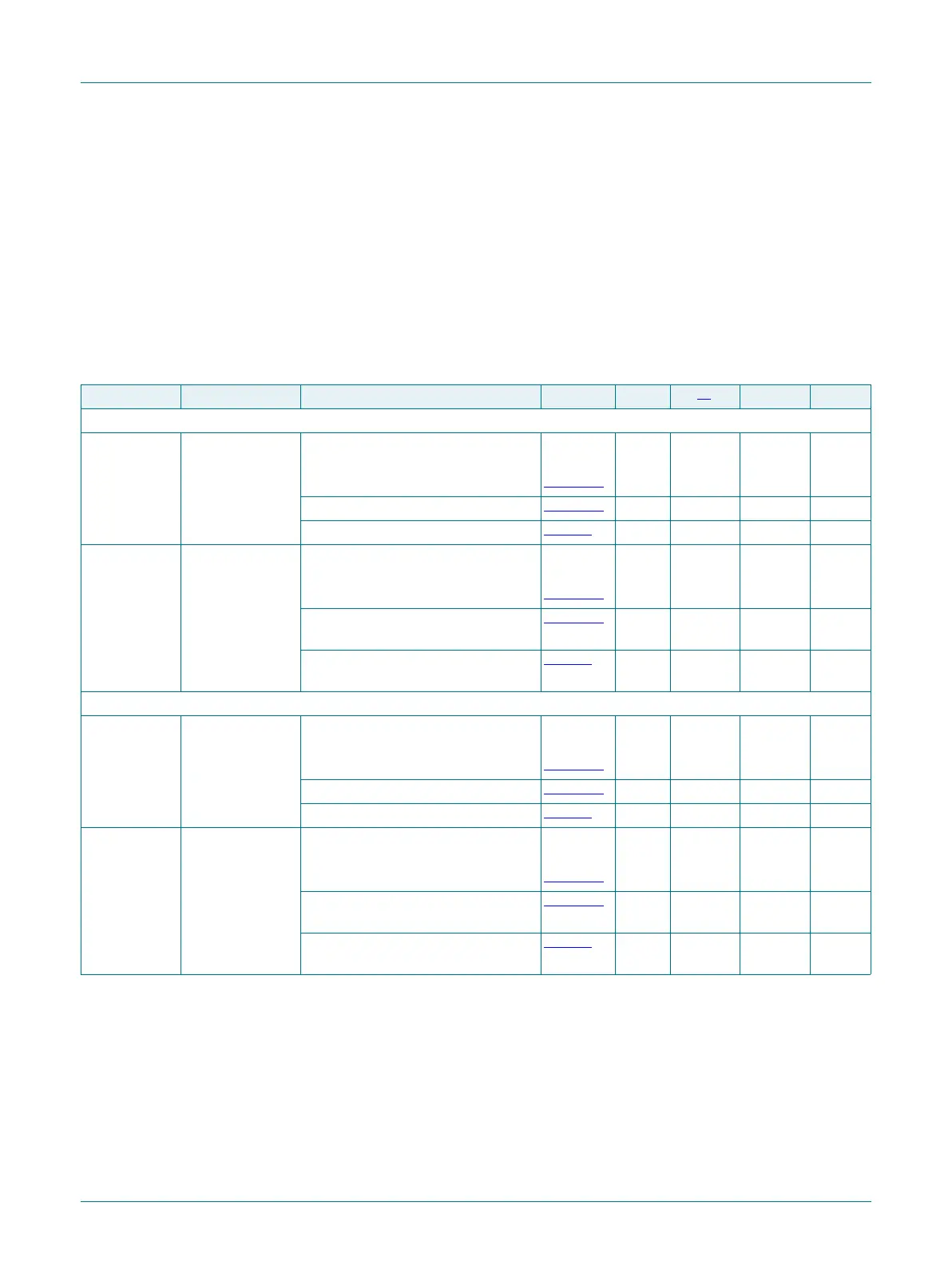
Table 14. Static characteristics: Power consumption in active mode
T
amb
=
40
C to +105
C, unless otherwise specified.1.62 V
V
DD
3.6 V.
Symbol Parameter Conditions Min Typ
[1]
Max Unit
ARM Cortex-M0+ in active mode; ARM Cortex-M4 in sleep mode
I
DD
supply current CoreMark code executed from
SRAMX; flash powered down:
CCLK = 12 MHz
[2][3][4][6][7]
-1.1- mA
CCLK = 48 MHz
[2][3][4][6][7]
-3.0- mA
CCLK = 96 MHz
[2][3][4][6]
-7.1- mA
I
DD
supply current CoreMark code executed from flash;
CCLK = 12 MHz; 1 system clock
flash access time.
[2][3][4][5][7]
-1.3- mA
CCLK = 48 MHz; 3 system clock
flash access time.
[2][3][4][5][7]
-3.6- mA
CCLK = 96 MHz; 7 system clock
flash access time.
[2][3][4][5]
-8.0- mA
ARM Cortex-M4 in active mode; ARM Cortex-M0+ in sleep mode
I
DD
supply current CoreMark code executed from
SRAMX; flash powered down:
CCLK = 12 MHz
[2][3][4][6][7]
-1.3- mA
CCLK = 48 MHz
[2][3][4][6][7]
-3.9- mA
CCLK = 96 MHz
[2][3][4][6]
-9.3- mA
I
DD
supply current CoreMark code executed from flash;
CCLK = 12 MHz; 1 system clock
flash access time.
[2][3][4][5][7]
-1.5- mA
CCLK = 48 MHz; 3 system clock
flash access time.
[2][3][4][5][7]
-4.6- mA
CCLK = 96 MHz; 7 system clock
flash access time.
[2][3][4][5]
-9.9- mA

 Loading...


