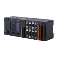
No. Signal No. Signal
1 AIN0+ 11 AIN0-
2 AIN1+ 12 AIN1-
3 AIN2+ 13 AIN2-
4 AIN3+ 14 AIN3-
5 AGND 15 AGND
6 AIN4+ 16 AIN4-
7 AIN5+ 17 AIN5-
8 AIN6+ 18 AIN6-
9 AIN7+ 19 AIN7-
10 AGND 20 AGND
3-5-6
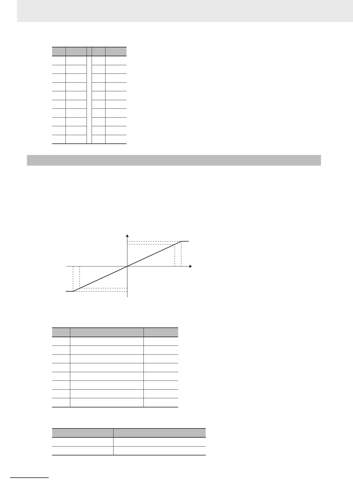
Analog Input Data
This section describes the correspondence between input analog signals and analog input data.
The graph shows that a voltage between -10 to 10 V is converted to data between 80D2 and 7F2E
hex (-32,558 to 32,558).
When a negative voltage is input, it is expressed as the two’
s complement (hexadecimal).
-10 V-10.064 V
1
0 V10.064 V
0000 (0)
7FFF (32,768)
7F2E (32,558)
80D2 (-32,558)
Converted data
Hexadecimal (Decimal)
8000 (-32,768)
0 V
Voltage
Analog input data is stored in the upper 16 bits of the following register.
T
o use a register value, divide it by 2
16
by using the program.
Input Register Bit position
AIN0 Gate3[i].Chan[0].ADCAmp[0] [31:16]
AIN1 Gate3[i].Chan[0].ADCAmp[1] [31:16]
AIN2 Gate3[i].Chan[0].ADCAmp[2] [31:16]
AIN3 Gate3[i].Chan[0].ADCAmp[3] [31:16]
AIN4 Gate3[i].Chan[1].ADCAmp[0] [31:16]
AIN5 Gate3[i].Chan[1].ADCAmp[1] [31:16]
AIN6 Gate3[i].Chan[1].ADCAmp[2] [31:16]
AIN7 Gate3[i].Chan[1].ADCAmp[3] [31:16]
The following table shows the conversion timing of analog input.
Input Conversion timing
AIN0, AIN1, AIN4, AIN5 At the rising edge of the phase clock
AIN2, AIN3, AIN6, AIN7 At the falling edge of the phase clock
3 Configuration Units
3-56
CK3M-series Programmable Multi-Axis Controller User's Manual Hardware (O036)
 Loading...