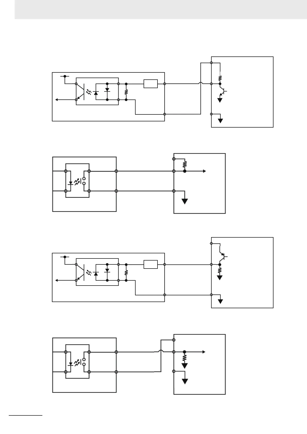
• Input circuit diagram (V430-F ⇔ External device) when NPN connected
Code reader
NPN device
+
V
GND
COM_IN
INPUT
・
TRIG
・
DEFAULT
・
NEW MASTER
CLC
CLC = Current Limiting Circuit
• Output circuit diagram (V430-F ⇔ External device) when NPN connected
NPN device
GND
COM_OUT
OUTPUT
・
OUTPUT1
・
OUTPUT2
・
OUTPUT3
+
V
Input
Code reader
• Input circuit diagram (V430-F ⇔ External device) when PNP connected
COM_IN
INPUT
・
TRIG
・
DEFAULT
・
NEW MASTER
CLC
CLC = Current Limiting Circuit
+
V
GND
Code reader
PNP device
• Output circuit diagram (V430-F ⇔ External device) when PNP connected
COM_OUT
OUTPUT
・
OUTPUT1
・
OUTPUT2
・
OUTPUT3
GND
+
V
Input
Code reader
PNP device
2 Controlling Operation and Data Output with Parallel
2 - 4
V430-F Series Autofocus Multicode Reader User Manual for Communication Settings

 Loading...