6-8
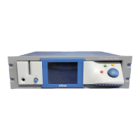
TECHNICAL DATA Orban Model 8400
A valid remote signal is a momentary pulse of current flowing through remote signal
pins. Current must flow consistently for 50msec for the signal to be interpreted as valid.
Generally, the 8400 will respond to the most recent control operation whether it came
from the front panel, remote interface, or RS-232.
Component-Level Description:
After being current limited by resistors, the GPI control signals are applied to two
quad optoisolators, U28, 30, and then to the control circuitry.
The RS232 ports are buffered by octal drivers U14, 17.
U28, 30 and U14, 17 are socketed for easy field replacement in the event of over-
load. All other circuitry is surface-mount and is not field-repairable.
2. Color LCD Display
The color LCD is a passive-matrix quarter-VGA panel. The CPU addresses it by memory
mapping.
The backlight on the display has a finite lifetime (ordinarily a few years of continuous
operation). Therefore, the 8400 always implements a screen-saver timeout. You will
maximize the life of this costly component by setting the screen-saver timeout as short as
practical.
Input Circuits
This circuitry interfaces the analog and digital inputs to the DSP. The analog input stages
scale and buffer the input audio level to match it to the analog-to-digital (A/D) converter.
The A/D converts the analog input audio to digital audio. The digital input receiver ac-
cepts AES/EBU-format digital audio signals from the digital input connector and sample
rate-converts them as necessary. The digital audio from the A/D and SRC is transmitted
to the DSP.
1. Analog Input Stages
Located on input/output board
The RF-filtered left and right analog input signals are each applied to a floating-balanced
amplifier that has an adjustable (digitally controlled) gain. Analog switches set the gain.
The outputs of a latch set the state of the switches. By writing data to the latch, the con-
trol circuits set the gain according to what the user specifies from the front panel controls.
The gain amplifier’s output feeds a circuit that scales, balances, and DC-biases the signal.
This circuit feeds an RC low-pass filter that applies the balanced signal to the analog-to-
digital (A/D) converter.