EasyManua.ls Logo

Renesas R8C series User Manual

Renesas R8C series
341 pages
To Next Page IconTo Next Page
To Previous Page IconTo Previous Page
Page #104 background imageLoading...
Page #104 background image
R8C/1A Group, R8C/1B Group 12. Interrupts
Rev.1.30 Dec 08, 2006 Page 86 of 315
REJ09B0252-0130
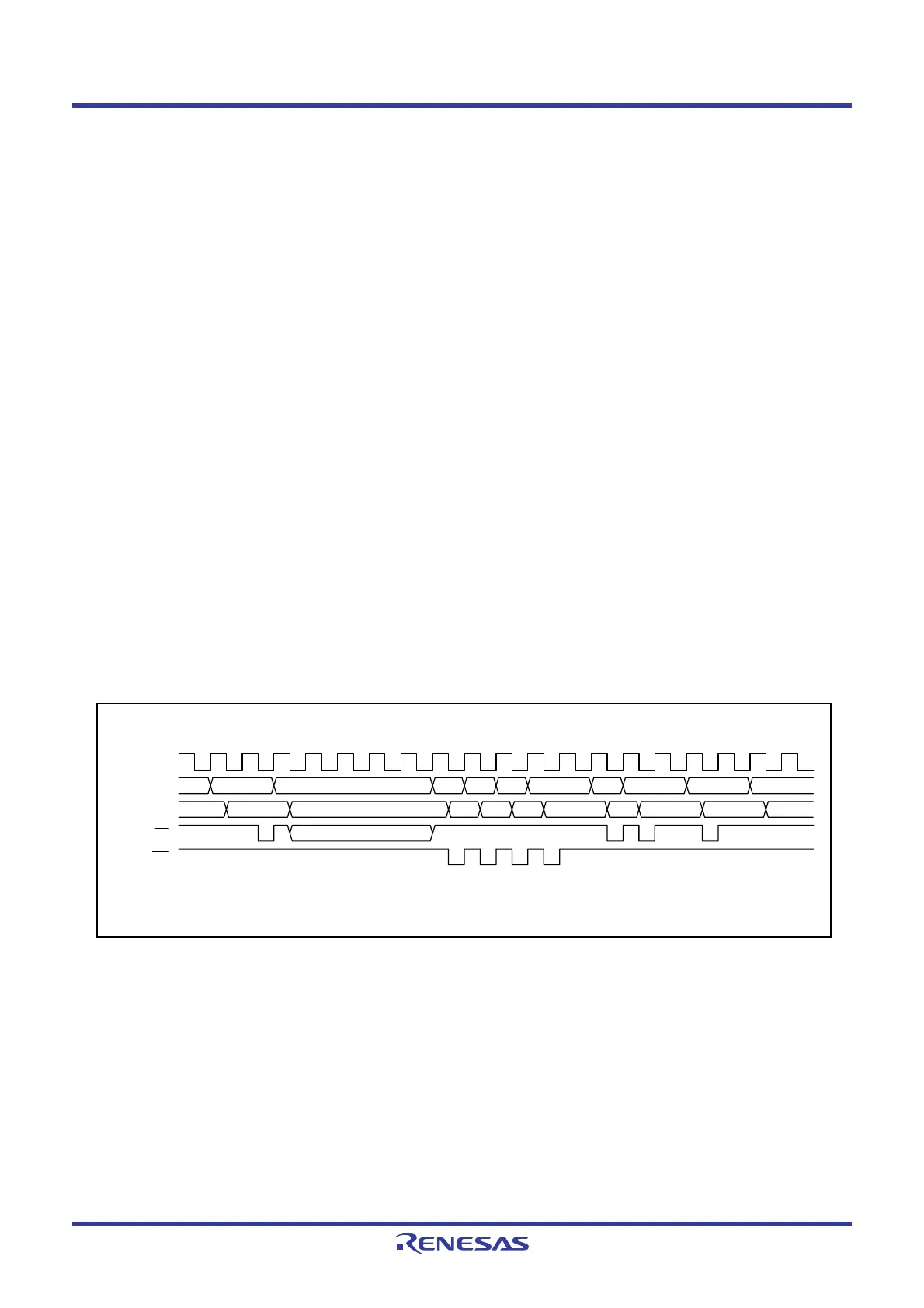
12.1.6.4 Interrupt Sequence
An interrupt sequence is performed between an interrupt request acknowledgement and interrupt routine
execution.
When an interrupt request is generated while an instruction is being executed, the CPU determines its interrupt
priority level after the instruction is completed. The CPU starts the interrupt sequence from the following cycle.
However, for the SMOVB, SMOVF, SSTR, or RMPA instruction, if an interrupt request is generated while the
instruction is being executed, the MCU suspends the instruction to start the interrupt sequence. The interrupt
sequence is performed as indicated below. Figure 12.5 shows the Time Required for Executing Interrupt
Sequence.
(1) The CPU gets interrupt information (interrupt number and interrupt request level) by reading address
00000h. The IR bit for the corresponding interrupt is set to 0 (interrupt not requested).
(2) The FLG register is saved to a temporary register
(1)
in the CPU immediately before entering the
interrupt sequence.
(3) The I, D, and U flags in the FLG register are set as follows:
The I flag is set to 0 (interrupts disabled).
The D flag is set to 0 (single-step interrupt disabled).
The U flag is set to 0 (ISP selected).
However, the U flag does not change state if an INT instruction for software interrupt number 32 to 63
is executed.
(4) The CPU’s internal temporary register
(1)
is saved to the stack.
(5) The PC is saved to the stack.
(6) The interrupt priority level of the acknowledged interrupt is set in the IPL.
(7) The starting address of the interrupt routine set in the interrupt vector is stored in the PC.
After the interrupt sequence is completed, instructions are executed from the starting address of the interrupt
routine.
NOTE:
1. This register cannot be used by user.
Figure 12.5 Time Required for Executing Interrupt Sequence
1234567891011 12 13 14 15 16 17 18 19 20
CPU clock
Address bus
Data bus
RD
WR
Address
0000h
Undefined
Undefined
Undefined
Interrupt
information
SP-2 SP-1 SP-4 SP-3 VEC VEC+1 VEC+2 PC
SP-2
contents
SP-1
contents
SP-4
contents
SP-3
contents
VEC
contents
VEC+1
contents
VEC+2
contents
The undefined state depends on the instruction queue buffer. A read cycle occurs when the instruction queue buffer is
ready to acknowledge instructions.

Table of Contents

Question and Answer IconNeed help?

Do you have a question about the Renesas R8C series and is the answer not in the manual?

Renesas R8C series Specifications

General IconGeneral
BrandRenesas
ModelR8C series
CategoryComputer Hardware
LanguageEnglish

Summary

Notice

Overview of R8C/1A and R8C/1B Groups

Applications

Lists various application areas for electric household appliances, office equipment, and industrial uses.

Performance Overview

Outlines the functions and specifications for R8C/1A and R8C/1B groups.

Notes Regarding These Materials

General Precautions in the Handling of MPU/MCU Products

Handling of Unused Pins

Guidance on handling unused pins to prevent noise induction and potential malfunctions in LSI operation.

Processing at Power-on

Explains the indeterminate states of internal circuits and pins during power supply until reset completion.

Prohibition of Access to Reserved Addresses

States that accessing reserved addresses is prohibited to maintain LSI operation integrity and future expansion.

Clock Signals

Provides instructions on stabilizing clock signals after reset and during program execution.

Differences between Products

Highlights that type numbers within the same group may have differing internal memory and layout patterns.

How to Use This Manual

Purpose and Target Readers

Defines the manual's purpose and the intended audience for understanding hardware functions and electrical characteristics.

Notation of Numbers and Symbols

Register, Bit, and Pin Names Notation

Explains how register, bit, and pin names are referred to using symbols in the text.

Number Notation Conventions

Details the use of 'b' for binary and 'h' for hexadecimal, with no suffix for decimal numbers.

Register Notation Conventions

List of Abbreviations and Acronyms

Special Function Registers (SFRs)

Programmable I/O Ports

Functions of Programmable I/O Ports

Explains how PDi_j bits control I/O ports and the structure of Pi registers, including latch and pin state reading.

Effect on Peripheral Functions

Describes how programmable I/O ports function for peripheral operations, referencing pin name information.

Pins Other Than Programmable I/O Ports

Illustrates the configuration of specific I/O pins that are not programmable, such as RESET and MODE.

Resets

Processor Mode

Bus

Clock Generation Circuit

Notes on Clock Generation Circuit

Covers stop mode, wait mode, oscillation stop detection, and selecting oscillation constants.

Protection

Interrupts

Interrupt Overview

Provides an overview of interrupt types, maskable vs. non-maskable interrupts, and priority.

INT Interrupt

Details the INT0 and INT1 interrupts, including input filters, polarity selection, and registers.

Key Input Interrupt

Explains the key input interrupt generation by pins K10-K13, its use as a wake-up function, and related registers.

Address Match Interrupt

Describes the address match interrupt for debugging, its generation, and associated registers.

Peripheral Function Interrupt

Explains peripheral function interrupts as maskable interrupts generated by internal MCU functions.

Interrupt Control

Details enabling/disabling maskable interrupts and setting priorities using I flag, IPL, and ILVL bits.

Watchdog Timer

Count Source Protection Mode Disabled

Describes watchdog timer specifications when count source protection mode is disabled, using CPU clock.

Count Source Protection Mode Enabled

Details watchdog timer specifications when count source protection mode is enabled, using low-speed oscillator.

Timers

Timer X

Details Timer X, an 8-bit timer with prescaler, covering its modes and associated registers.

Timer Z

Describes Timer Z, an 8-bit timer with prescaler, covering its modes and associated registers.

Timer C

Explains Timer C, a 16-bit timer with input capture and output compare modes, and its registers.

Serial Interface

Clock Synchronous Serial I/O Mode

Explains the clock synchronous serial I/O mode, its configurations, and associated registers.

Clock Asynchronous Serial I/O (UART) Mode

Describes the UART mode for asynchronous serial data transmission and reception, including bit rate settings.

Notes on Serial Interface

Provides important notes on reading and writing serial interface registers, error detection, and data handling.

Clock Synchronous Serial Interface

Mode Selection for Clock Synchronous Serial Interface

Outlines the four modes of the clock synchronous serial interface, including SSU, I2C, communication, and serial modes.

Clock Synchronous Serial I/O with Chip Select (SSU)

Details SSU specifications, including transfer data format, operating modes, master/slave devices, and pins.

I2C Bus Interface

Explains the I2C bus interface specifications, block diagram, timing examples, and associated registers.

A/D Converter

One-Shot Mode for A/D Converter

Details the one-shot mode where a single pin's analog voltage is converted once.

Repeat Mode for A/D Converter

Explains the repeat mode for continuous A/D conversion of a selected pin.

Sample and Hold Function for A/D Converter

Discusses the sample and hold function and its impact on conversion rate and accuracy.

A/D Conversion Cycles

Lists the timing requirements for A/D conversion in various modes and resolutions.

Internal Equivalent Circuit of Analog Input Block

Illustrates the internal equivalent circuit of the analog input block, useful for circuit design.

Inflow Current Bypass Circuit

Explains the configuration and application of inflow current bypass circuits for noise reduction.

Output Impedance of Sensor under A/D Conversion

Addresses the impact of sensor output impedance on A/D conversion accuracy and charging time.

Notes on A/D Converter

Provides essential notes on register access, voltage settings, operating modes, and prohibited instructions.

Flash Memory

Flash Memory Overview

Introduces flash memory rewrite operations in CPU, serial, and parallel I/O modes.

Flash Memory Map

Details the flash memory block diagrams for R8C/1A and R8C/1B groups, showing ROM and data flash areas.

Functions to Prevent Flash Memory Rewriting

Explains ID code check and ROM code protect functions to safeguard flash memory from unauthorized access.

CPU Rewrite Mode for Flash Memory

Describes rewriting the user ROM area directly from the CPU using software commands.

Electrical Characteristics

Absolute Maximum Ratings

Lists critical limits for voltage, power dissipation, and temperature to prevent device damage.

Recommended Operating Conditions

Specifies voltage, clock frequency, and temperature ranges for ensuring reliable device operation.

Usage Notes

Notes on Clock Generation Circuit

Covers precautions for stop mode, wait mode, oscillation stop detection, and selecting oscillation constants.

Notes on Interrupts

Provides notes on reading address 00000h, SP setting, external/key input interrupts, and watchdog timer.

Precautions on Timers

Details precautions for Timer X and Timer Z to ensure correct operation and prevent issues like incorrect counting.

Notes on Serial Interface

Provides notes on serial interface register access, error handling, and data transfer for UART and synchronous modes.

Precautions on Clock Synchronous Serial Interface

Covers precautions for accessing registers and selecting signal pins in clock synchronous serial I/O modes.

Notes on A/D Converter

Provides notes on register operations, voltage settings, operating modes, and prohibited instructions for the A/D converter.

Notes on Flash Memory

Details important notes regarding CPU rewrite mode, operating speed, prohibited instructions, and interrupt handling for flash memory.

Notes on On-Chip Debugger

Package Dimensions

Connection Examples for Serial Writer and On-Chip Debugging Emulator

Example of Oscillation Evaluation Circuit

Related product manuals