R8C/1A Group, R8C/1B Group 13. Watchdog Timer
Rev.1.30 Dec 08, 2006 Page 104 of 315
REJ09B0252-0130
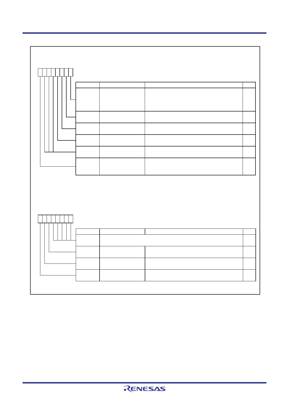
Figure 13.2 Registers OFS and WDC
Watchdog Timer Control Register
Symbol Address After Reset
WDC
000Fh 00X11111b
Bit Symbol Bit Name Function RW
b3 b2 b1 b0
RW
High-order bits of w atchdog timer—
(b4-b0)
RW
—
(b5)
00
b7 b6 b5 b4
RW
Reserved bit Set to 0. When read, the content is undefined.
RO
WDC7
—
(b6)
Reserved bit Set to 0.
Prescaler select bit 0 : Divided by 16
1 : Divided by 128
Option Function Select Register
(1)
Symbol Address Before Shipment
OFS
0FFFFh FFh
(2)
Bit Symbol Bit Name Function RW
NOTES :
1.
2.
CSPROINI
Count source protection
mode after reset select
bit
0 : Count source protect mode enabled after reset
1 : Count source protect mode disabled after reset
RW
—
(b6-b4)
Reserved bits Set to 1.
RW
0 : ROM code protect disabled
1 : ROMCP1 enabled
RW
ROMCP1
ROM code protect bit 0 : ROM code protect enabled
1 : ROM code protect disabled
RW
0 : Starts w atchdog timer automatically after reset.
1 : Watchdog timer is inactive after reset.
1
The OFS register is on the flash memory. Write to the OFS register w ith a program.
—
(b1)
RW
Reserved bit Set to 1.
ROMCR
ROM code protect
disabled bit
111
b7 b6 b5 b4
If the block including the OFS register is erased, FFh is set to the OFS register.
b3 b2 b1 b0
WDTON RW
Watchdog timer start
select bit
 Loading...


