R8C/1A Group, R8C/1B Group 14. Timers
Rev.1.30 Dec 08, 2006 Page 126 of 315
REJ09B0252-0130
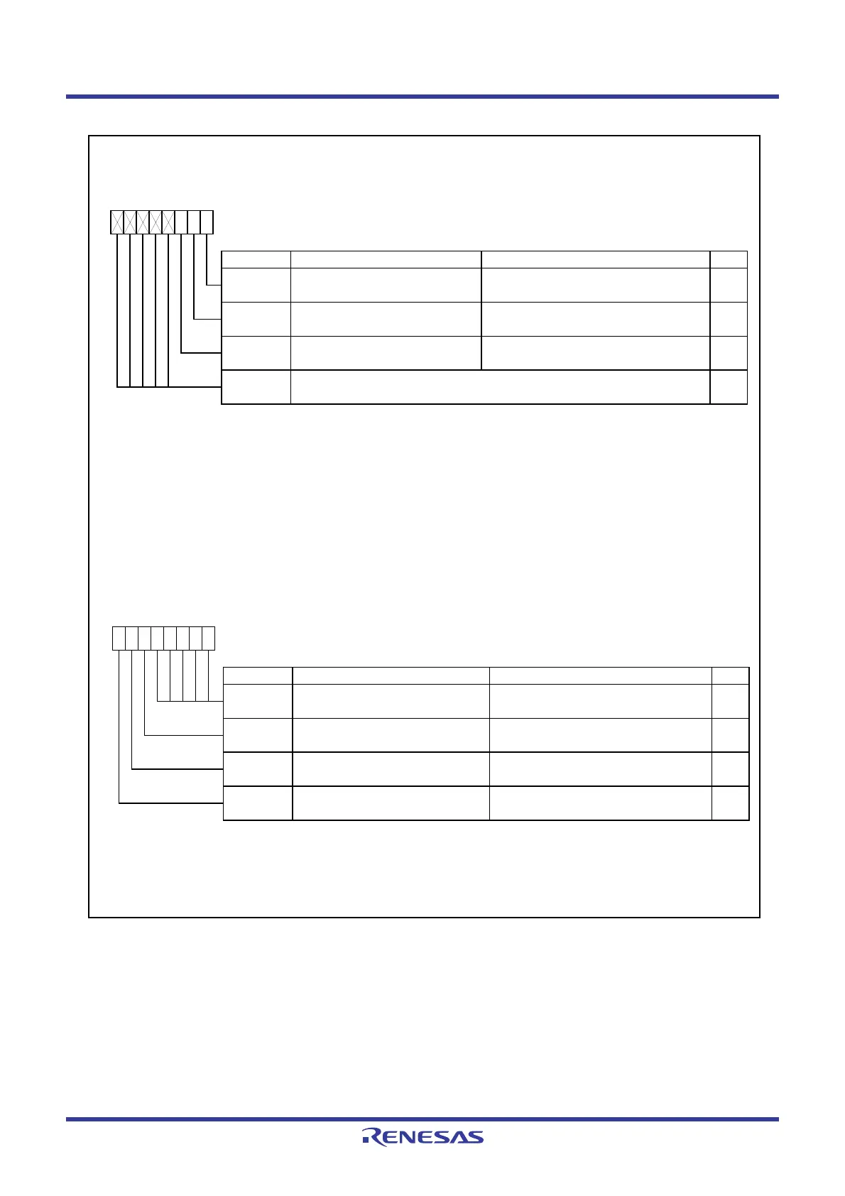
Figure 14.14 Registers TZOC and PUM
Timer Z Output Control Register
(3)
Symbol Address After Reset
TZOC
008Ah 00h
Bit Symbol Bit Name Function RW
NOTES :
1.
2.
3. When executing an instruction w hich changes this register w hen the TZOS bit is set to 1 (during count), the TZOS
bit is automatically set to 0 (one-shot stop) if the count is completed w hile the instruction is being executed. If this
causes problems, execute an instruction w hich changes the contents of this register w hen the TZOS bit is set to 0
(one-shot stop).
b3 b2 b1 b0
TZOS RW
0
b7 b6 b5 b4
Timer Z one-shot start bit
(1)
0 : One-shot stops.
1 : One-shot starts.
Reserved bit Set to 0.
RW
—
(b1)
RW
Timer Z programmable w aveform
generation output sw itch bit
(2)
0 : Outputs programmable w aveform.
1 : Outputs value in P1_3 port register.
TZOCNT
This bit is set to 0 w hen the output of a one-shot w aveform is completed. If the TZS bit in the TZMR register w as set
to 0 (count stops) to stop the w aveform output during one-shot w aveform output, set the TZOS bit to 0.
This bit is enabled only w hen operating in programmable w aveform generation mode.
Nothing is assigned. If necessary, set to 0.
When read, the content is 0.
—
(b7-b3)
—
Timer Z Waveform Output Control Register
Symbol Address After Reset
PUM
0084h 00h
Bit Symbol Bit Name Function RW
INT0
____
pin one-shot trigger control 0 : INT0
____
pin one-shot trigger disabled
bit (timer Z)
(2)
1 : INT0
____
pin one-shot trigger enabled
INT0
____
pin one-shot trigger polarity
select bit (timer Z)
(1)
NOTES :
1.
2.
RW
RW
INOSEG RW
0 : Falling edge trigger
1 : Rising edge trigger
INOSTG
Timer Z output level latch
0
Reserved bits Set to 0.
TZOPL
RW
b7 b6 b5 b4
00
The INOSEG bit is enabled only w hen the INT0PL bit in the INTEN register is set to 0 (one edge).
Set the INOSTG bit to 1 after setting the INT0EN bit in the INTEN register and the INOSEG bit in the PUM register.
0
b3 b2
Function varies depending on operating
mode.
b1 b0
0
—
(b4-b0)
 Loading...


