R8C/1A Group, R8C/1B Group 15. Serial Interface
Rev.1.30 Dec 08, 2006 Page 156 of 315
REJ09B0252-0130
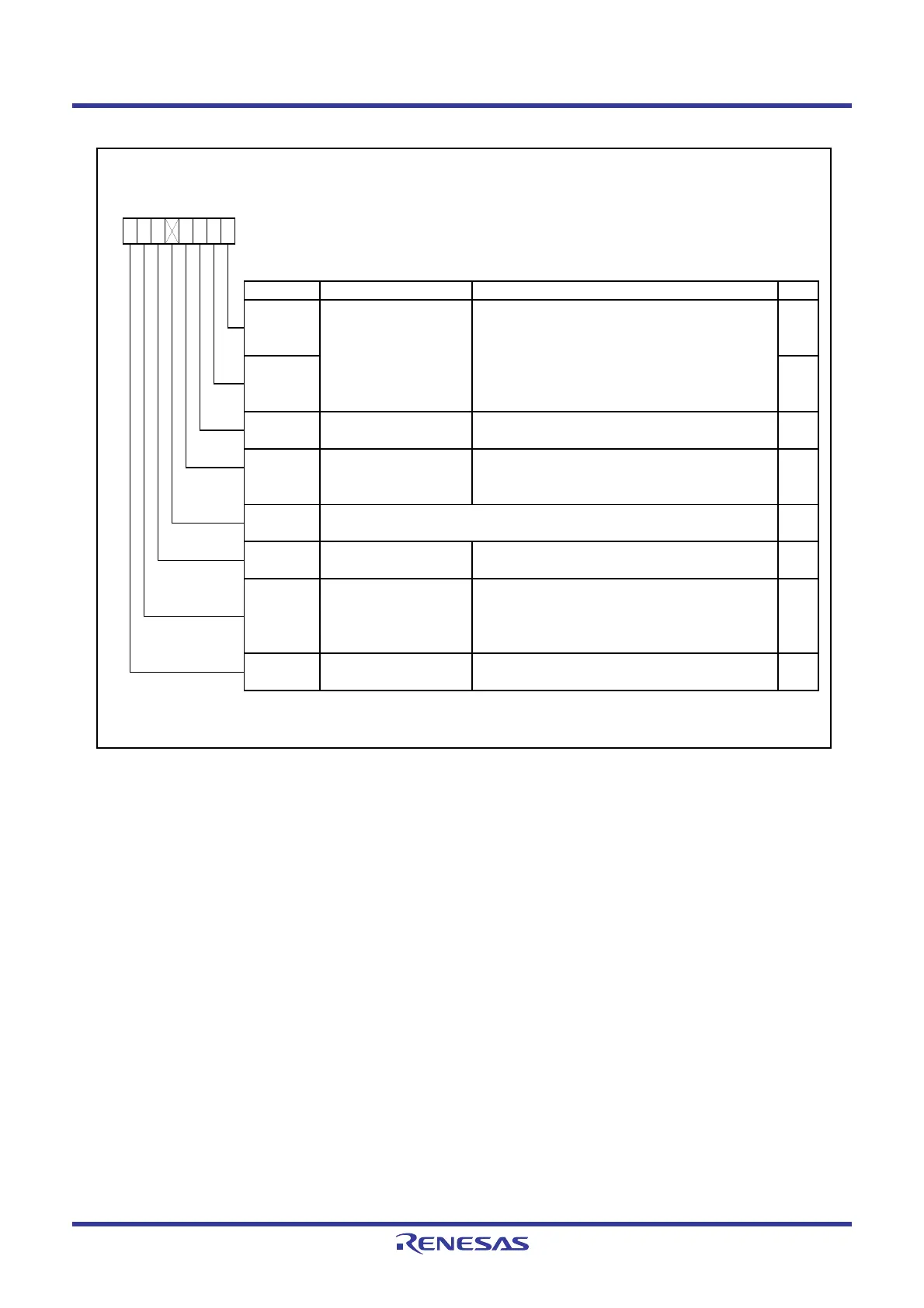
Figure 15.5 Registers U0C0 to U1C0
UARTi Transmit / Receive Control Register 0 (i = 0 or 1)
Symbol Address After Reset
U0C0
00A4h 08h
U1C0
00ACh 08h
Bit Symbol Bit Name Function RW
NOTE :
1.
b3 b2
TXEPT
b1 b0
0
CLK0
b7 b6 b5 b4
RW
RO
—
(b4)
—
Reserved bit
CLK1 RW
BRG count source select
bits
(1)
b1 b0
0 0 : Selects f1.
0 1 : Selects f8.
1 0 : Selects f32.
1 1 : Do not set.
RW
NCH
CLK polarity select bit 0 : Transmit data is output at falling edge of transfer
clock and receive data is input at rising edge.
1 : Transmit data is output at rising edge of transfer
clock and receive data is input at falling edge.
Set to 0.
Transmit register empty
flag
0 : Data in transmit register (during transmit)
1 : No data in transmit register (transmit completed)
Nothing is assigned. If necessary, set to 0.
When read, the content is 0.
—
(b2)
CKPOL RW
RW
If the BRG count source is sw itched, set the UiBRG register again.
RW
Data output select bit 0 : TXDi pin is for CMOS output.
1 : TXDi pin is for N-channel open drain output.
UFORM
Transfer format select bit 0 : LSB first
1 : MSB first
 Loading...


