R8C/1A Group, R8C/1B Group 16. Clock Synchronous Serial Interface
Rev.1.30 Dec 08, 2006 Page 178 of 315
REJ09B0252-0130
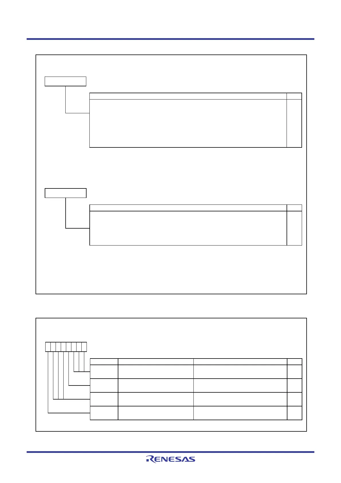
Figure 16.8 Registers SSTDR and SSRDR
Figure 16.9 PMR Register
SS Transmit Data Register
(1)
Symbol Address After Reset
SSTDR
00BEh FFh
RW
NOTE :
1.
b5 b4 b2
Ref er to
16.2.8.1 Accessing Registers Associated with Clock Synchronous Serial I/O with Chip Select
for
more information.
RW
b1
Function
Store the transmit data.
The stored transmit data is transferred to the SSTRSR register and transmission is started
w hen it is detected that the SSTRSR register is empty.
When the next transmit data is w ritten to the SSTDR register during the data transmission from
the SSTRSR register, the data can be transmitted continuously.
When the MLS bit in the SSMR register is set to 1 (transfer data w ith LSB-first), the data in
w hich MSB and LSB are reversed is read, after w riting to the SSTDR register.
b0b3b7 b6
SS Receive Data Register
(2)
Symbol Address After Reset
SSRDR
00BFh FFh
RW
NOTES :
1.
2.
The SSRDR register retains the data received before an overrun error occurs (ORER bit in the SSSR register set to 1
(overrun error)). When an overrun error occurs, the receive data may contain errors and therefore should be
discarded.
Store the receive data.
(1)
The receive data is transferred to the SSRDR register and the receive operation is completed
w hen 1 byte of data has been received by the SSTRSR register. At this time, the next receive
operation is possible. Continuous reception is possible using registers SSTRSR and SSRDR.
RO
Function
Ref er to
16.2.8.1 Accessing Registers Associated with Clock Synchronous Serial I/O with Chip Select
for
more information.
b7 b6 b5 b4 b3 b2 b1 b0
Port Mode Registe
Symbol Address After Reset
PMR
00F8h 00h
Bit Symbol Bit Name Function RW
000
b7 b6 b5 b4 b3 b2
0
b1
0
b0
0
RW
Reserved bits
SSISEL
SSI signal pin select bit
—
(b2-b0)
—
(b6-b4)
IICSEL RW
0 : Selects SSU function.
1 : Selects I
2
C bus function.
Set to 0.
0 : P3_3 pin is used for SSI00 pin.
1 : P1_6 pin is used for SSI01 pin.
Set to 0.
RW
Reserved bits
SSU / I
2
C bus sw itch bit
RW
 Loading...


