R8C/1A Group, R8C/1B Group 16. Clock Synchronous Serial Interface
Rev.1.30 Dec 08, 2006 Page 177 of 315
REJ09B0252-0130
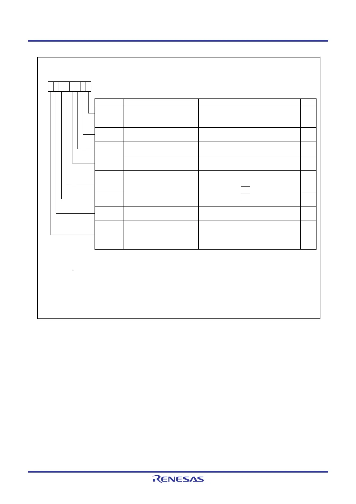
Figure 16.7 SSMR2 Register
SS Mode Register 2
(5)
Symbol Address After Reset
SSMR2
00BDh 00h
Bit Symbol Bit Name Function RW
SCS
____
pin open drain output select
0 : CMOS output
bit
1 : NMOS open drain output
SCS
_____
pin select bits
(2)
b5 b4
0 0 : Functions as port.
0 1 : Functions as SCS
____
input pin.
1 0 : Functions as SCS
____
output pin.
(3)
1 1 : Functions as SCS
____
output pin.
(3)
NOTES :
1.
2.
3.
4.
5.
b0
Ref er to
16.2.2.1 Relationship between Data I/O Pin and SS Shift Register
for information on combinations of
data I/O pins.
The SCS
____
pin functions as a port, regardless of the values of bits CSS0 and CSS1 w hen the SSUMS bit is set to 0
SCKS
SSCK pin select bit 0 : Functions as port.
1 : Functions as serial clock pin.
RW
b3 b2 b1b7 b6 b5 b4
SOOS
SCKOS
SSUMS
CSOS
0 : Clock synchronous communication mode
1 : Four-w ire bus communication mode
SSCK pin open drain output
select bit
0 : CMOS output
1 : NMOS open drain output
CSS1
Clock synchronous serial I/O w ith
chip select mode select bit
(1)
Serial data open drain output
select bit
(1)
0 : CMOS output
1 : NMOS open drain output
CSS0
RW
RW
RW
RW
RW
RW
Ref er to
16.2.8.1 Accessing Registers Associated with Clock Synchronous Serial I/O with Chip Select
for
more information.
The BIDE bit is disabled when the SSUMS bit is set to 0 (clock synchronous communication mode).
RWBIDE
Bidirectional mode enable bit
(1, 4)
0 : Standard mode (communication using 2
pins of data input and data output)
1 : Bidirectional mode (communication using
1 pin of data input and data output)
s
t
unct
ons as t
e
nput p
n
e
ore start
ng trans
er.
(clock synchronous communication mode).
 Loading...


