R8C/1A Group, R8C/1B Group 16. Clock Synchronous Serial Interface
Rev.1.30 Dec 08, 2006 Page 176 of 315
REJ09B0252-0130
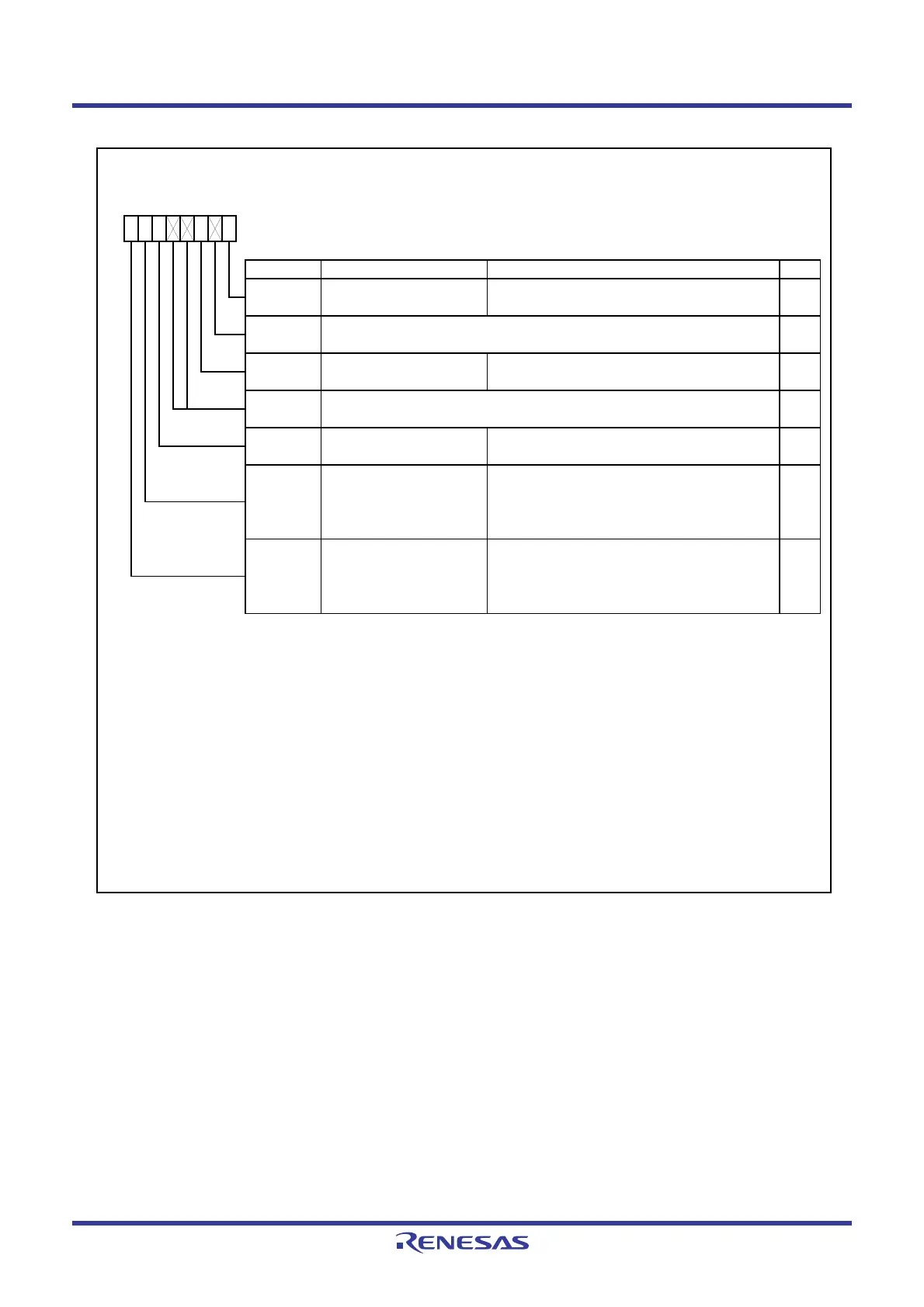
Figure 16.6 SSSR Register
SS Status Register
(7)
Symbol Address After Reset
SSSR
00BCh 00h
Bit Symbol Bit Name Function RW
NOTES :
1.
2.
3.
4.
5.
6.
7. Refer to
16.2.8.1 Accessing Registers Associated with Clock Synchronous Serial I/O with Chip Select
for
more information.
Indicates w hen overrun errors occur and receive completes by error reception. If the next serial data receive
operation is completed w hile the RDRF bit is set to 1 (data in the SSRDR register), the ORER bit is set to 1. After the
ORER bit is set to 1 (overrun error), transmit and receive operations are disabled w hile the bit remains 1.
When the serial communication is started w hile the SSUMS bit in the SSMR2 register is set to 1 (four-w ire bus
communication mode) and the MSS bit in the SSCRH register is set to 1 (operates as master device), the CE bit is set
to 1 if “L” is applied to the SCS pin input. When the SSUMS bit in the SSMR2 register is set to 1 (four-w ire bus
communication mode), the MSS bit in the SSCRH register is set to 0 (operates as slave device) and the SCS pin input
changes the level from “L” to “H” during transfer, the CE bit is set to 1.
The TDRE bit is set to 1 w hen the TE bit in the SSER re
ister is set to 1
transmit enabled
.
CE
—
Bits TEND and TDRE are set to 0 w hen w ritin
data to the SSTDR re
ister.
Overrun error flag
(1)
0 : No overrun errors generated
1 : Overrun errors generated
(3)
TEND
Transmit end
(1, 5)
0 : The TDRE bit is set to 0 w hen transmitting
the last bit of transmit data.
1 : The TDRE bit is set to 1 w hen transmitting
the last bit of transmit data.
RW
RW
RW
RW
—
Conflict error flag
(1)
0 : No conflict errors generated
1 : Conflict errors generated
(2)
RDRF
Receive data register full
(1,4)
—
(b1)
Nothing is assigned. If necessary, set to 0.
When read, the content is 0.
0 : No data in SSRDR register
1 : Data in SSRDR register
ORER
—
(b4-b3)
b3 b2 b1b7 b6 b5 b4 b0
Writing 1 to CE, ORER, RDRF, TEND, or TDRE bit is invalid. To set any of these bits to 0, first read 1 then w rite 0.
The RDRF bit is set to 0 w hen readin
out the data from the SSRDR re
ister.
Nothing is assigned. If necessary, set to 0.
When read, the content is 0.
TDRE
Transmit data empty
(1, 5, 6)
0 : Data is not transferred from registers SSTDR to
SSTRSR.
1 : Data is transferred from registers SSTDR to
SSTRSR.
RW
 Loading...


