R8C/1A Group, R8C/1B Group 16. Clock Synchronous Serial Interface
Rev.1.30 Dec 08, 2006 Page 187 of 315
REJ09B0252-0130
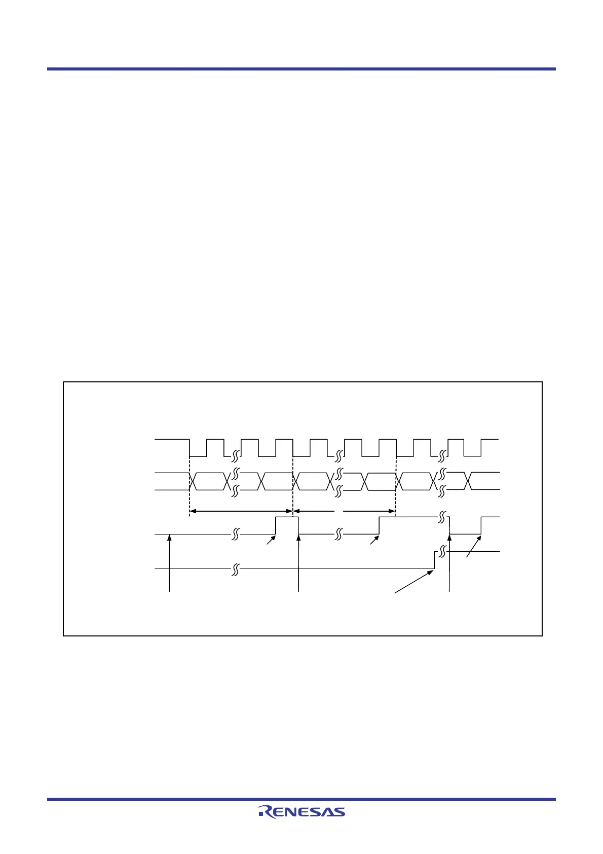
16.2.5.3 Data Reception
Figure 16.15 shows an Example of Clock Synchronous Serial I/O with Chip Select Operation for Data
Reception (Clock Synchronous Communication Mode).
During data reception clock synchronous serial I/O with chip select operates as described below. When clock
synchronous serial I/O with chip select is set as the master device, it outputs a synchronous clock and inputs
data. When clock synchronous serial I/O with chip select is set as a slave device, it inputs data synchronized
with the input clock.
When clock synchronous serial I/O with chip select is set as a master device, it outputs a receive clock and starts
receiving by performing dummy read of the SSRDR register.
After 8 bits of data are received, the RDRF bit in the SSSR register is set to 1 (data in the SSRDR register) and
receive data is stored in the SSRDR register. When the RIE bit in the SSER register is set to 1 (RXI and OEI
interrupt requests enabled), the RXI interrupt request is generated. If the SSDR register is read, the RDRF bit is
automatically set to 0 (no data in the SSRDR register).
Read the receive data after setting the RSSTP bit in the SSCRH register to 1 (after receiving 1 byte of data, the
receive operation is completed). Clock synchronous serial I/O with chip select outputs a clock for receiving 8
bits of data and stops. After that, set the RE bit in the SSER register to 0 (receive disabled) and the RSSTP bit to
0 (receive operation is continued after receiving the 1 byte of data) and read the receive data. If the SSRDR
register is read while the RE bit is set to 1 (receive enabled), a receive clock is output again.
When the 8th clock rises while the RDRF bit is set to 1, the ORER bit in the SSSR register is set to 1 (overrun
error: OEI) and the operation is stopped. When the ORER bit is set to 1, receive cannot be performed. Confirm
that the ORER bit is set to 0 before restarting receive.
Figure 16.16 shows a Sample Flowchart of Data Reception (MSS = 1) (Clock Synchronous Communication
Mode).
Figure 16.15 Example of Clock Synchronous Serial I/O with Chip Select Operation for Data
Reception (Clock Synchronous Communication Mode)
SSCK
b0
SSI
• SSUMS = 0 (clock synchronous communication mode), CPHS = 0 (data download at
even edges) and CPOS bit = 0 (“H” when clock stops)
b0b7
1 frame
RDRF bit in
SSSR register
0
1
RSSTP bit in
SSCRH register
0
1
Dummy read in
SSRDR register
Processing
by program
RXI interrupt request
generation
b0
b7 b7
1 frame
RXI interrupt request
generation
Read data in SSRDR
register
Read data in
SSRDR register
Set RSSTP bit to 1
RXI interrupt request
generation
 Loading...


