R8C/1A Group, R8C/1B Group 16. Clock Synchronous Serial Interface
Rev.1.30 Dec 08, 2006 Page 188 of 315
REJ09B0252-0130
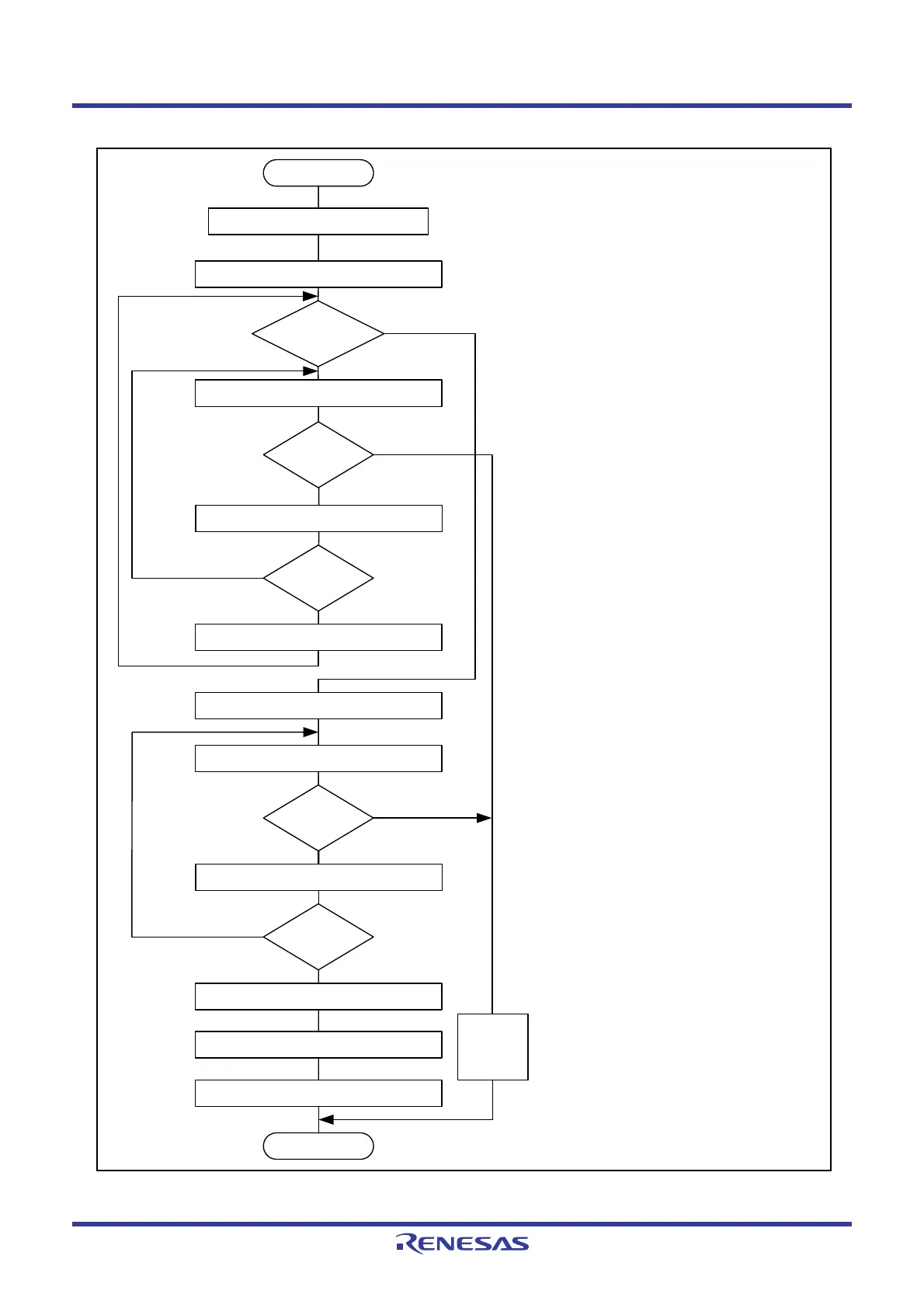
Figure 16.16 Sample Flowchart of Data Reception (MSS = 1) (Clock Synchronous Communication
Mode)
Start
Initialization
Dummy read of SSRDR register
Read receive data in SSRDR register
Read ORER bit in SSSR register
Last data
received?
Read RDRF bit in SSSR register
RDRF = 1 ?
No
Yes
Yes
No
No
Yes
(1)
(2)
(3)
(1) After setting each register in the clock synchronous
serial I/O with chip select register, a dummy read of
the SSRDR register is performed and the receive
operation is started.
(2) Determine whether it is the last 1 byte of data to be
received. If so, set to stop after the data is received.
(3) If a receive error occurs, perform error.
(6) Processing after reading the ORER bit. Then set
the ORER bit to 0. Transmission/reception cannot
be restarted while the ORER bit is set to 1.
(4) Confirm that the RDRF bit is set to 1. If the RDRF
bit is set to 1, read the receive data in the SSRDR
register. When the SSRDR register is read, the
RDRF bit is automatically set to 0.
ORER = 1 ?
End
Read receive data in SSRDR register
Read ORER bit in SSSR register
Read RDRF in SSSR register
RDRF = 1 ?
No
Yes
ORER = 1 ?
SSER register RE bit ← 0
SSCRH register RSSTP bit ← 0
SSCRH register RSSTP bit ← 1
Overrun
error
processing
No
Yes
(4)
(5)
(6)
(7)
(7) Confirm that the RDRF bit is set to 1. When the
receive operation is completed, set the RSSTP bit to
0 and the RE bit to 0 before reading the last 1 byte
of data. If the SSRDR register is read before setting
the RE bit to 0, the receive operation is restarted
again.
(5)Before the last 1 byte of data is received, set the
RSSTP bit to 1 and stop after the data is
received.
 Loading...


