R8C/1A Group, R8C/1B Group 16. Clock Synchronous Serial Interface
Rev.1.30 Dec 08, 2006 Page 207 of 315
REJ09B0252-0130
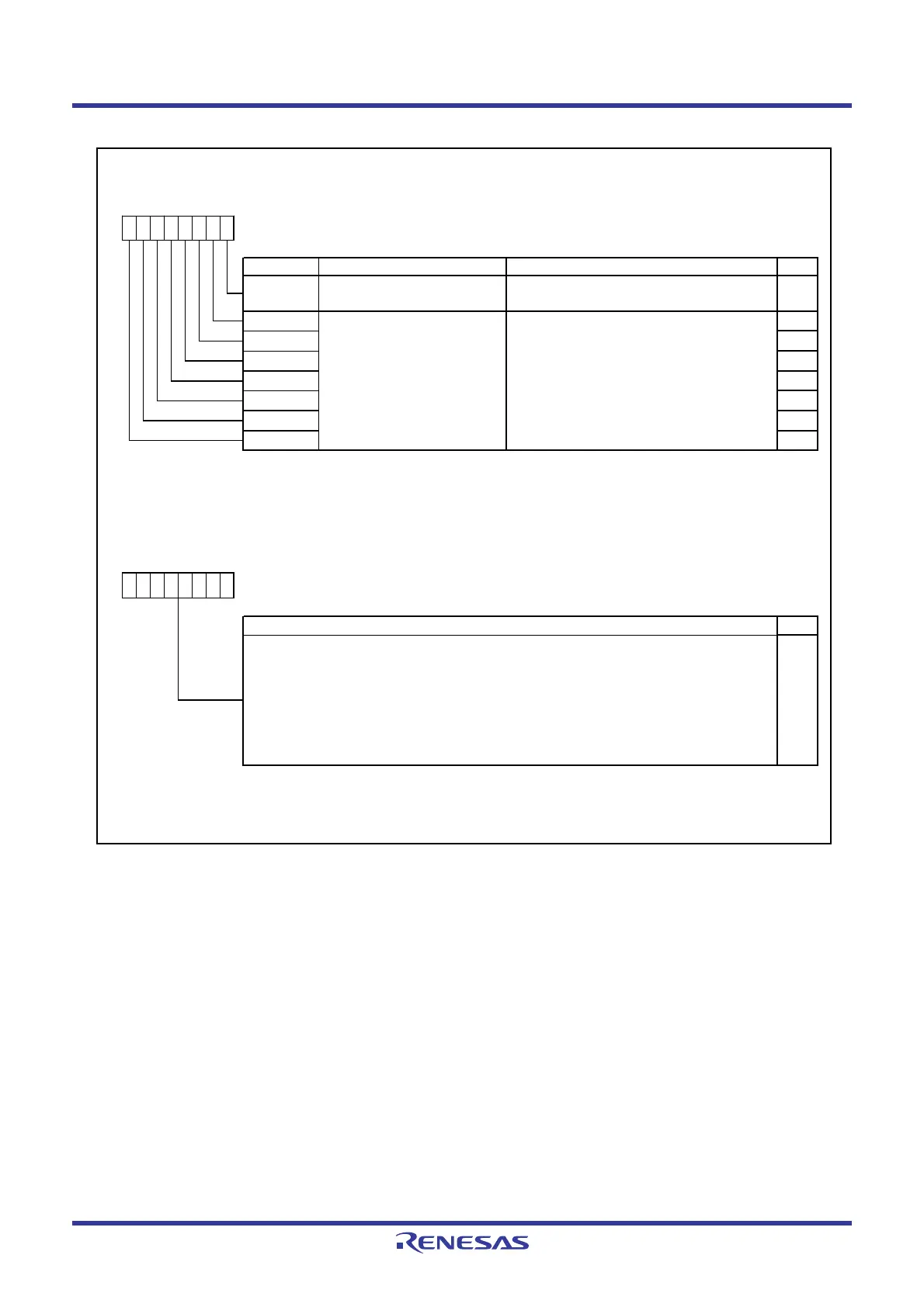
Figure 16.29 Registers SAR and ICDRT
Slave Address Register
(1)
Symbol Address After Reset
SAR
00BDh 00h
Bit Symbol Bit Name Function RW
NOTE :
1.
b7 b6 b0b1b5 b3 b2b4
SVA1
FS
Format select bit 0 : I
2
C bus format
1 : Clock synchronous serial format
RW
Ref er to
16.3.8.1 Accessing of Registers Associated with I
2
C bus Interface
for more information.
RW
Slave address 6 to 0 Set an address different from that of the other
slave devices w hich are connected to the I
2
C
bus.
When the 7 high-order bits of the first frame
transmitted after the starting condition match
bits SVA0 to SVA6 in slave mode of the I
2
C
bus format, the MCU operates as a slave
device.
RW
RW
RW
RW
SVA2
SVA0
RW
SVA3
SVA6
SVA5
SVA4
RW
IIC bus Transmit Data Register
(1)
Symbol Address After Reset
ICDRT
00BEh FFh
RW
NOTE :
1. Refer to
16.3.8.1 Accessing of Registers Associated with I
2
C bus Interface
for more information.
b0b7 b6 b5 b4 b3 b2 b1
RW
Function
Store transmit data
When it is detected that the ICDRS register is empty, the stored transmit data item is
transferred to the ICDRS register and data transmission starts.
When the next transmit data item is w ritten to the ICDRT register during transmission of the
data in the ICDRS register, continuous transmit is enabled. When the MLS bit in the ICMR
register is set to 1 (data transferred LSB-first) and after the data is w ritten to the ICDRT
register, the MSB-LSB inverted data is read.
 Loading...


