R8C/1A Group, R8C/1B Group 16. Clock Synchronous Serial Interface
Rev.1.30 Dec 08, 2006 Page 208 of 315
REJ09B0252-0130
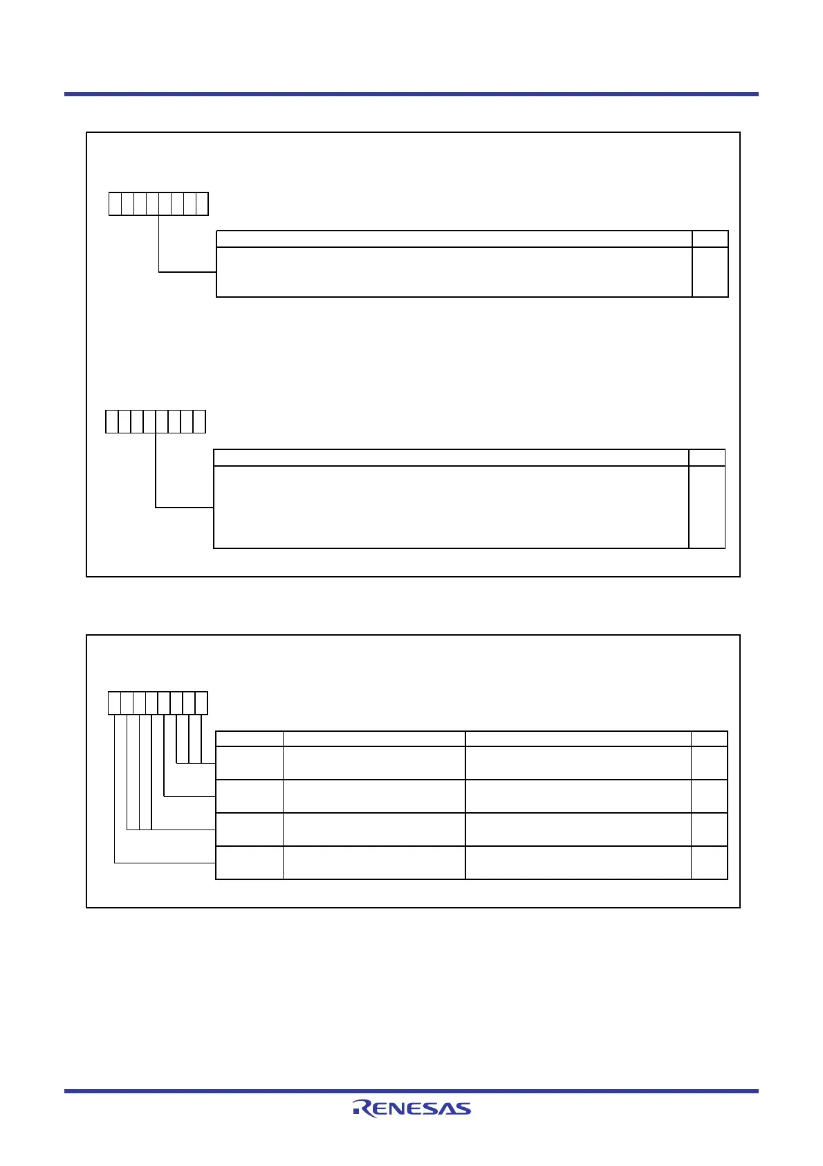
Figure 16.30 Registers ICDRR and ICDRS
Figure 16.31 PMR Register
IIC bus Receive Data Register
(1)
Symbol Address After Reset
ICDRR 00BFh FFh
RW
NOTE :
1. Refer to
16.3.8.1 Accessing of Registers Associated with I
2
C bus Interface
for more information.
b7 b6 b5 b4 b3 b2 b1 b0
Store receive data
When the ICDRS register receives 1 byte of data, the receive data is transferred to the ICDRR
register and the next receive operation is enabled.
RO
Function
IIC bus Shift Register
Symbol
ICDRS
RW
b7 b6 b5 b4 b3 b2 b1 b0
This register is used to transmit and receive data.
The transmit data is transferred from registers ICRDT to ICDRS and data is transmitted from
the SDA pin w hen transmitting.
After 1 byte of data is received, data is transferred from registers ICDRS to ICDRR w hile
receiving.
—
Function
Port Mode Registe
Symbol Address After Reset
PMR
00F8h 00h
Bit Symbol Bit Name Function RW
IICSEL RW
0 : Selects SSU function.
1 : Selects I
2
C bus function.
Set to 0.
0 : P3_3 pin is used for SSI00 pin.
1 : P1_6 pin is used for SSI01 pin.
Set to 0.
RW
Reserved bits
SSU / I
2
C bus sw itch bit
RW
b0
0
RW
Reserved bits
SSISEL
SSI signal pin select bit
—
(b2-b0)
—
(b6-b4)
b3 b2
0
b1
0
b7 b6 b5 b4
000
 Loading...


