R8C/1A Group, R8C/1B Group 19. Electrical Characteristics
Rev.1.30 Dec 08, 2006 Page 283 of 315
REJ09B0252-0130
NOTES:
1. V
CC = 2.7 to 5.5V, VSS = 0V at Ta = -20 to 85 °C / -40 to 85 °C, unless otherwise specified.
2. 1t
CYC = 1/f1(s)
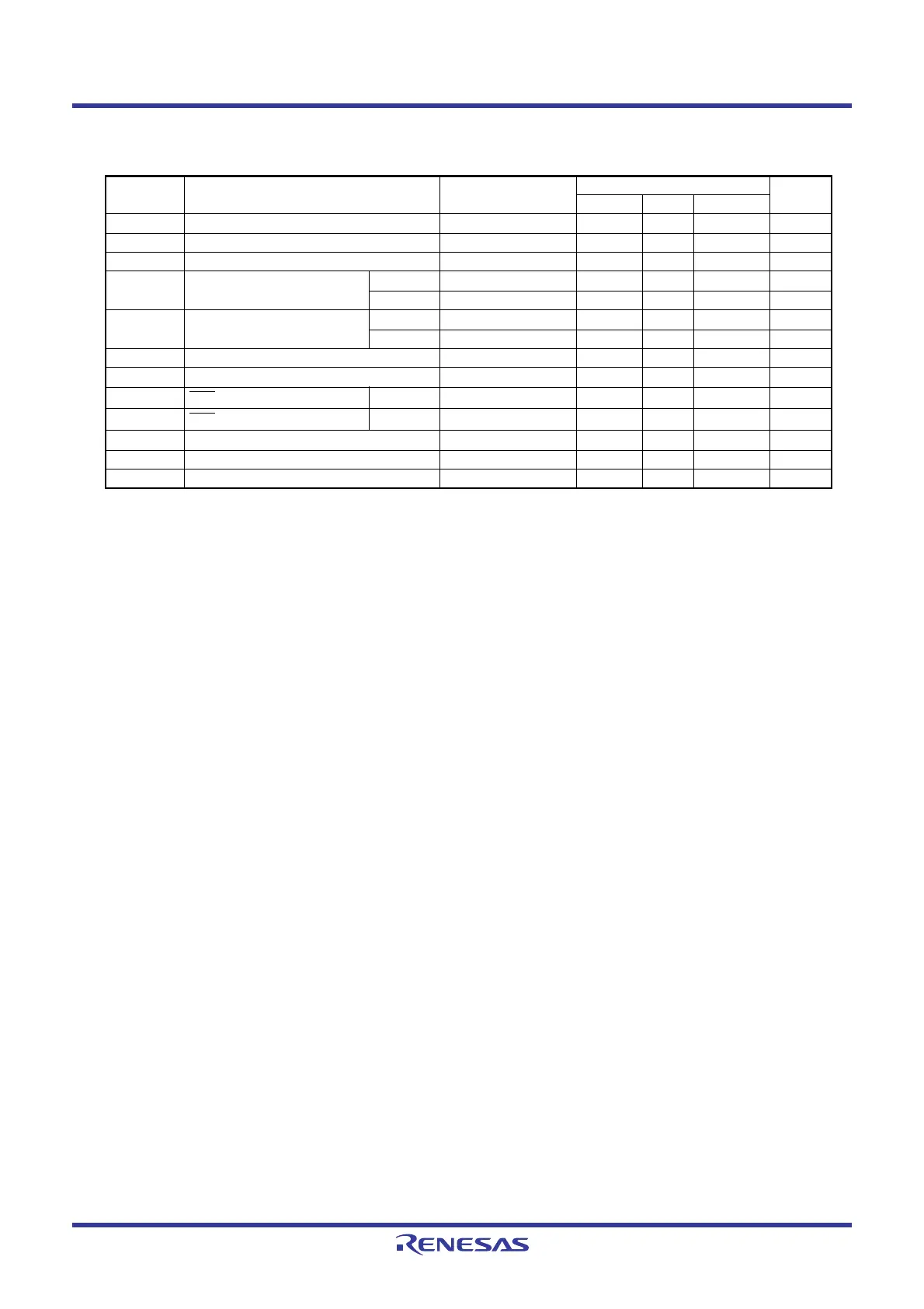
Table 19.12 Timing Requirements of Clock Synchronous Serial I/O with Chip Select
(1)
Symbol Parameter Conditions
Standard
Unit
Min. Typ. Max.
t
SUCYC SSCK clock cycle time 4 −−
tCYC
(2)
tHI SSCK clock “H” width 0.4 − 0.6 tSUCYC
tLO SSCK clock “L” width 0.4 − 0.6 tSUCYC
tRISE SSCK clock rising time Master −− 1
t
CYC
(2)
Slave −− 1 µs
t
FALL SSCK clock falling time Master −− 1
t
CYC
(2)
Slave −− 1 µs
t
SU SSO, SSI data input setup time 100 −− ns
t
H SSO, SSI data input hold time 1 −−
tCYC
(2)
tLEAD
SCS setup time
Slave 1t
CYC+50 −− ns
tLAG
SCS hold time
Slave 1t
CYC+50 −− ns
tOD SSO, SSI data output delay time −− 1
t
CYC
(2)
tSA SSI slave access time −−1.5tCYC+100 ns
t
OR SSI slave out open time −−1.5tCYC+100 ns
 Loading...


