R8C/1A Group, R8C/1B Group 5. Programmable I/O Ports
Rev.1.30 Dec 08, 2006 Page 28 of 315
REJ09B0252-0130
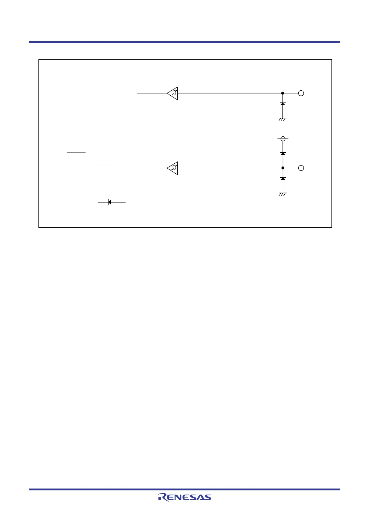
Figure 5.4 Configuration of I/O Pins
MODE
MODE signal input
(Note 1)
RESET
RESET signal input
(Note 1)
NOTE :
1. symbolizes a parasitic diode.
Ensure the input voltage to each port will not exceed VCC.
 Loading...


