R8C/1A Group, R8C/1B Group 5. Programmable I/O Ports
Rev.1.30 Dec 08, 2006 Page 27 of 315
REJ09B0252-0130
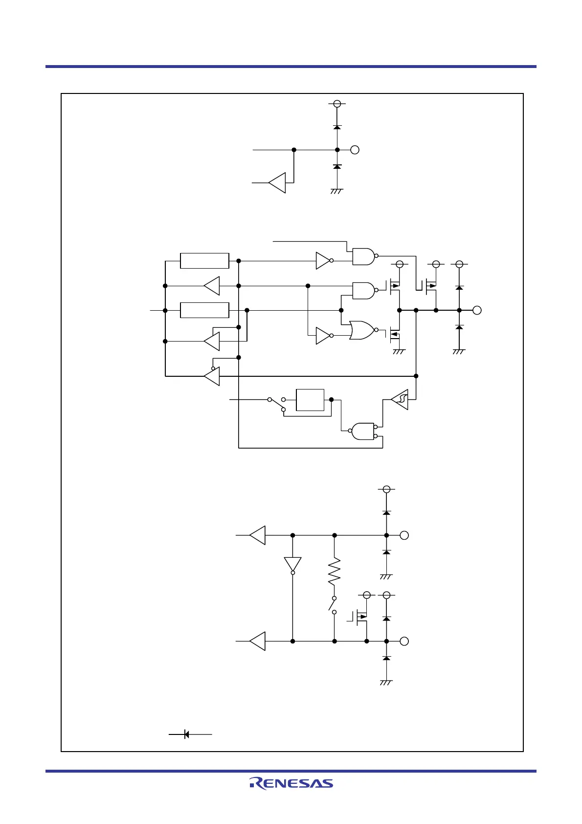
Figure 5.3 Configuration of Programmable I/O Ports (3)
P4_5
Input to individual peripheral function
Port latch
Direction
register
Data bus
Pull-up selection
Digital
filter
P4_6/XIN
Data bus
Clocked inverter
(1)
P4_7/XOUT
Data bus
(Note 2)
(Note 3)
NOTES:
1. When CM05 = 1, CM10 = 1, or CM13 = 0, the clocked inverter is cut off.
2. When CM10 = 1 or CM13 = 0, the feedback resistor is disconnected.
3. When CM05 = CM13 = 1 or CM10 = CM13 = 1, this pin is pulled up.
4. symbolizes a parasitic diode.
Ensure the input voltage to each port does not exceed VCC.
P4_2
Data bus
Vref of A/D converter
(Note 4)
(Note 4)
(Note 4)
(Note 4)
 Loading...


