R8C/1A Group, R8C/1B Group 5. Programmable I/O Ports
Rev.1.30 Dec 08, 2006 Page 30 of 315
REJ09B0252-0130
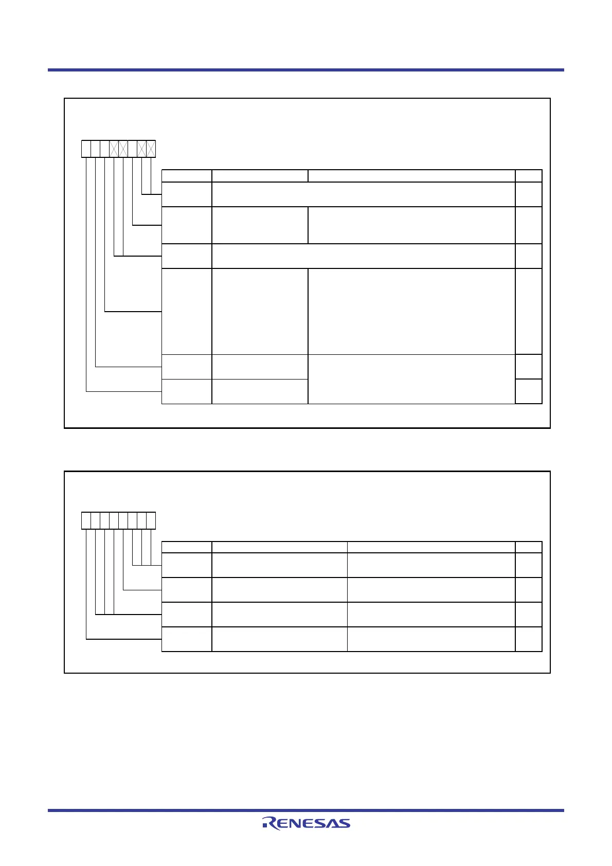
Figure 5.7 P4 Register
Figure 5.8 PMR Register
Port P4 Register
Symbol Address After Reset
P4
00E8h Undefined
Bit Symbol Bit Name Function RW
Nothing is assigned. If necessary, set to 0 (“L” level).
When read, the content is 0.
The level of the pin can be read by reading the bit.
0 : “L” level
1 : “H” level
Nothing is assigned. If necessary, set to 0 (“L” level).
When read, the content is 0.
The pin level of any I/O port w hich is set to input mode
can be read by reading the corresponding bit in this
register. The pin level of any I/O port w hich is set to
output mode can be controlled by w riting to the
corresponding bit in this register.
0 : “L” level
1 : “H” level
RW
Port P4_6 bit
R
Port P4_2 bit
R
—
The level of the pin can be read by reading the bit.
0 : “L” level
1 : “H” level
R
—
Port P4_7 bit
Port P4_5 bit
P4_5
—
(b1-b0)
P4_7
P4_6
b7 b6 b5 b4 b3 b2 b1
—
(b4-b3)
b0
P4_2
Port Mode Registe
Symbol Address After Reset
PMR
00F8h 00h
Bit Symbol Bit Name Function RW
000
b7 b6 b5 b4 b3 b2
0
b1
0
b0
0
RW
Reserved bits
SSISEL
SSI signal pin select bit
—
(b2-b0)
—
(b6-b4)
IICSEL RW
0 : Selects SSU function.
1 : Selects I
2
C bus function.
Set to 0.
0 : P3_3 pin is used for SSI00 pin.
1 : P1_6 pin is used for SSI01 pin.
Set to 0.
RW
Reserved bits
SSU / I
2
C bus sw itch bit
RW
 Loading...


