R8C/1A Group, R8C/1B Group 5. Programmable I/O Ports
Rev.1.30 Dec 08, 2006 Page 31 of 315
REJ09B0252-0130
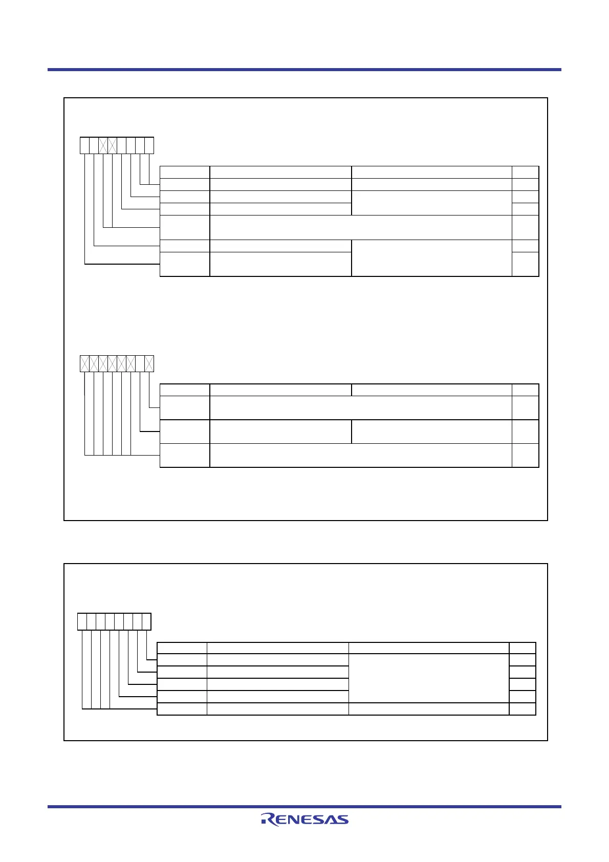
Figure 5.9 Registers PUR0 and PUR1
Figure 5.10 DRR Register
Pull-Up Control Register 0
Symbol Address After Reset
PUR0
00FCh 00XX0000b
Bit Symbol Bit Name Function RW
NOTE :
1.
RW
When this bit is set to 1 (pulled up), the pin w hose direction bit is set to 0 (input mode) is pulled up.
PU07
PU06
RW
RW
RWP1_4 to P1_7 pull-up
(1)
PU02
—
(b5-b4)
PU03
b3 b2 b1
0
b0
0
(b1-b0)
b7 b6 b5 b4
P1_0 to P1_3 pull-up
(1)
Reserved bits
P3_4 to P3_5, and P3_7 pll-up
(1)
—
P3_3 pull-up
(1)
RW0 : Not pulled up
1 : Pulled up
Nothing is assigned. If necessary, set to 0.
When read, the content is undefined.
0 : Not pulled up
1 : Pulled up
Set to 0.
Pull-Up Control Register 1
Symbol Address After Reset
PUR1
00FDh XXXXXX0Xb
Bit Symbol Bit Name Function RW
NOTE :
1.
—
PU11
P4_5 pull-up
(1)
0 : Not pulled up
1 : Pulled up
RW
—
(b7-b2)
Nothing is assigned. If necessary, set to 0.
When read, the content is undefined.
—
(b0)
Nothing is assigned. If necessary, set to 0.
When read, the content is undefined.
b7 b6 b5 b4 b0
—
When the PU11 bit is set to 1 (pulled up), and the PD4_5 bit is set to 0 (input mode), the P4_5 pin is
pulled up.
b3 b2 b1
Port P1 Drive Capacity Control Register
Symbol Address After Reset
DRR
00FEh 00h
Bit Symbol Bit Name Function RW
DRR0
DRR2
Set to 0.
b7 b6 b5 b4
0000
b3 b2 b1 b0
RWP1_2 drive capacity
DRR1 P1_1 drive capacity
RW
Set P1 N-channel output transistor drive
capacity.
0 : Low
1 : High
Reserved bits(b7-b4)
RWP1_0 drive capacity
DRR3 P1_3 drive capacity RW
RW
 Loading...


