R8C/1A Group, R8C/1B Group 10. Clock Generation Circuit
Rev.1.30 Dec 08, 2006 Page 60 of 315
REJ09B0252-0130
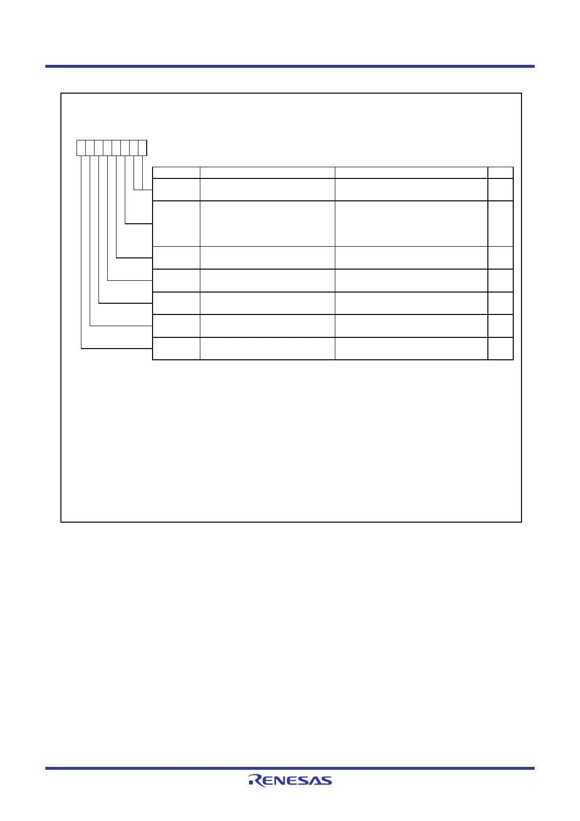
Figure 10.2 CM0 Register
System Clock Control Register 0
(1)
Symbol Address After Reset
CM0
0006h 68h
Bit Symbol Bit Name Function RW
NOTES :
1.
2.
3.
4.
5.
b7 b6 b5 b4 b3 b2 b1 b0
00100
—
(b1-b0)
Reserved bits Set to 0.
RW
CM02
WAIT peripheral function clock stop
bit
0 : Peripheral function clock does not stop
in w ait mode.
1 : Peripheral function clock stops in
w ait mode.
RW
—
(b3)
Reserved bit Set to 1.
RW
—
(b4)
Reserved bit Set to 0.
RW
CM05
Main clock (XIN-XOUT)
stop bit
(2,4)
0 : Main clock oscillates.
1 : Main clock stops.
(3)
RW
CM06
System clock division select bit 0
(5)
0 : CM16, CM17 enabled
1 : Divide-by-8 mode
RW
—
(b7)
Reserved bit Set to 0.
RW
When entering stop mode from high or medium speed mode, the CM06 bit is set to 1 (divide-by-8 mode).
Set the PRC0 bit in the PRCR register to 1 (w rite enable) before rew riting the CM0 register.
The CM05 bit stops the main clock w hen the on-chip oscillator mode is selected.
Do not use this bit to detect w hether the main clock is stopped. To stop the main clock, set the bits in the follow ing
order:
(a) Set bits OCD1 and OCD0 in the OCD register to 00b (oscillation stop detection function disabled).
(b) Set the OCD2 bit to 1 (selects on-chip oscillator clock).
To input an external clock, set the CM05 bit to 1 (main clock stops) and the CM13 bit in the CM1 register to 1 (XIN-
XOUT pin).
When the CM05 bit is set to 1 (main clock stops) and the CM13 bit in the CM1 register is set to 0 (P4_6, P4_7), P4_6
and P4_7 can be used as input ports.
 Loading...


