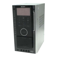
HCD-AZ33D
74
Pin No. Pin Name I/O Description
156 DVDD3 - Power supply terminal (+3.3V)
157 to 159
SMPTE_Y (7) to
SMPTE_Y (5)
O Digital video signal output terminal Not used
160 DVDD18 - Power supply terminal (+1.8V)
161 to 165
SMPTE_Y (4) to
SMPTE_Y (0)
O Digital video signal output terminal Not used
166 VCLK O Digital video output clock signal output terminal Not used
167 MIC I Microphone detection signal input terminal "H": microphone insert
168 TSD_M O Thermal shut down signal output to the coil/motor driver
169 MUTE O Muting signal output to the coil/motor driver
170 DVDD3 - Power supply terminal (+3.3V)
171 MUTE123 O Muting signal output to the coil/motor driver
172 REV O Loading motor drive signal output to the motor driver (reverse direction)
173 FWD O Loading motor drive signal output to the motor driver (forward direction)
174 DVDD18 - Power supply terminal (+1.8V)
175 RGB_SEL I RGB selection signal input terminal Not used
176 XDACS O Chip select signal output terminal Not used
177 WIDE O Squeeze/normal selection signal output to the video amplifi er "L": normasl, "H": squeeze
178 DVSS - Ground terminal
179 VBUS_OE O Power supply on/off control signal output terminal for USB section "L": power on
180 XMAMUTE O Muting request signal output terminal Not used
181 VBUS_OC I VBUS over current detection signal input terminal
182, 183 R/CR/PR, B/CB/PB O Component video signal output to the video amplifi er
184 DACVSSA - Ground terminal
185 Y/G O Chroma signal output to the video amplifi er
186 DACVDDA - Power supply terminal (+3.3V)
187 CVBS O Video signal output to the video amplifi er
188 DACVSSB - Ground terminal
189 C O Chroma signal output to the video amplifi er
190 DACVDDB - Power supply terminal (+3.3V)
191 Y O Y signal output to the video amplifi er
192 DACVSSC - Ground terminal
193 CIN O Compensation capacitor connection terminal
194 FS - Full scale adjustment terminal
195 VREF - Bandgap reference voltage terminal
196 DACVDDC - Power supply terminal (+3.3V)
197 ASDATA0 O Audio serial data output to the D/A converter
198 TRG_SW I Trigger detection switch input terminal
199 SCORE I Score signal input terminal
200 XVOICE I Voice signal input terminal
201 DIR_ERROR O Error signal output terminal Not used
202, 203 ASDATA1, ASDATA2 O Audio serial data output to the D/A converter
204 SPMCLK O Master clock signal output terminal for SPDIF Not used
205 SPDATA O Serial data output terminal for SPDIF Not used
206 SPLRCK O L/R sampling clock signal output terminal for SPDIF Not used
207 SPBLK O Bit clock signal output terminal for SPDIF Not used
208 DVDD3 - Power supply terminal (+3.3V)
209 ALRCK O L/R sampling clock signal output to the D/A converter
210 ABCK O Bit clock signal output to the D/A converter
211 ACLK O Master clock signal output to the D/A converter
212 ADIN I SPDIF audio digital signal input terminal Not used
213 DVDD18 - Power supply terminal (+1.8V)
214 ASDATA4 O Audio serial data output to the D/A converter
215 MC_DATA I Microphone serial data input terminal Not used
216 SPDIF O SPDIF audio digital signal output terminal
217 APLLVDD3 - Power supply terminal (+3.3V)