EasyManua.ls Logo

Sony HCD-AZ33D User Manual

Sony HCD-AZ33D
109 pages
To Next Page IconTo Next Page
Page #1 background imageLoading...
Page #1 background image
SERVICE MANUAL
Published by Sony Techno Create Corporation
Sony Corporation
Personal Audio Division
HCD-AZ33D
SPECIFICATIONS
DVD DECK RECEIVER
9-887-761-03
2007J05-1
©
2007.10
AEP Model
E Model
Australian Model
Ver. 1.2 2007.10
HCD-AZ33D is the ampli er, USB, disc player,
tape deck and tuner section in DHC-AZ33D.
DVD
Section
Model Name Using Similar Mechanism
NEW
DVD Mechanism Type
CDM86-DVBU101
Optical Pick-up Block Name
KHM-313CAB
Tape deck
Section
Model Name Using Similar Mechanism
NEW
Tape Transport Mechanism Type
CRP42603
This is system incorporates Dolby
1)
Digital, Dolby Pro Logic (II) adaptive
matrix surround decoder, and DTS
2)
DigitalSurround System.
1)
Manufactured under license from Dolby Laboratories.
“Dolby”, “Pro Logic”, and the double-D symbol are trademarks of Dolby Laboratories.
2)
“DTS” and “DTS Digital Surround” are registered trademarks of DTS, Inc.
“DTS” is a registered trademark of DTS, Inc. and “DTS 2.0 + Digital Out” is a
trademark of DTS, Inc.
DivX
@
is a video file compression technology, developed by DivX, Inc.
DivX, DivX Certified, and associated logos are trademarks of DivX, Inc. and
are used under license.
“WALKMAN” and “WALKMAN” logo are registered trademarks of Sony
Corporation.
MICROVAULT is a trademark of Sony Corporation.
MPEG Layer-3 audio coding technology and patents licensed from
Fraunhofer IIS and Thomson.
– Continued on next page –
Ampli er section
The following measured at AC 120, 127, 220, 240 V,
50/60 Hz
Power output (rated):
80 W + 80 W (4 Ω at 1 kHz, 1% THD)
RMS output power (reference):
100 W+ 100 W (per channel at 4 Ω, 1 kHz, 10%
THD)
Inputs
VIDEO/SAT IN (audio) (phono jacks):
voltage 250/450 mV, impedance
47 kilohms
MIC 1/MIC 2 (phone jacks):
sensitivity 1 mV, impedance
10 kilohms
Outputs
VIDEO/SAT OUT (audio) (phono jacks):
voltage 250 mV, impedance 1 kilohm
VIDEO OUT (phono jack):
max. output level 1 Vp-p, unbalanced,
Sync negative, load impedance
75 ohms
S VIDEO OUT (4-pin/mini-DIN jack):
Y: 1 Vp-p, unbalanced, Sync negative,
C: 0.286 Vp-p, load impedance
75 ohms
COMPONENT VIDEO OUT:
Y: 1 Vp-p, 75 ohms
P
B/CB: 0.7 Vp-p, 75 ohms
P
R/CR: 0.7 Vp-p, 75 ohms
DVD/USB DIGITAL OUT (Square optical connector
jack, rear panel):
Wavelength 660 nm
PHONES (stereo mini jack):
accepts headphones of 8 ohms or more
FRONT SPEAKER:
Use only the supplied speaker SS-AZ55D.
USB section
Supported audio le format
MP3 (MPEG 1 Audio Layer-3) Bit rate: 32 – 320
kbps*, VBR
Sampling frequencies:
32/44.1/48 kHz
(USB) port:
Maximum current: 500 mA
Video color system format
European and Russian models: PAL
Other models: NTSC and PAL
* 128 kbps or higher bit rate is recommended
Disc player section
System:
Compact disc and digital audio and video system
Laser:
Semiconductor laser (DVD:
λ=650 nm, CD: λ=790 nm)
Emission duration: continuous
Frequency response
DVD (PCM 48 kHz): 2 Hz – 22 kHz (±1dB)
CD: 2 Hz – 20 kHz (±0.5 dB)
Video color system format
European and Russian models: PAL
Other models: NTSC and PAL

Table of Contents

Question and Answer IconNeed help?

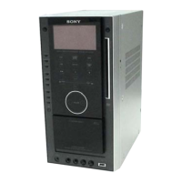
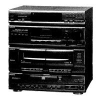
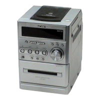
Do you have a question about the Sony HCD-AZ33D and is the answer not in the manual?

Sony HCD-AZ33D Specifications

General IconGeneral
BrandSony
ModelHCD-AZ33D
CategoryStereo System
LanguageEnglish

Summary

SPECIFICATIONS

Amplifier section

Details power output, inputs, and outputs for the amplifier section.

USB section

Information on supported audio file formats and bit rates for USB.

Disc player section

Details system, laser type, emission duration, and frequency response.

SELF DIAGNOSIS FUNCTION

Self-diagnosis Function

Explains the self-diagnosis feature and lists error codes.

General Power Requirements

Lists voltage and frequency requirements for different regions.

SERVICING NOTES

NOTES ON HANDLING THE OPTICAL PICK-UP BLOCK OR BASE UNIT

Precautions for handling sensitive components like optical pick-up blocks.

UNLEADED SOLDER

Information on unleaded solder characteristics and usage.

RELEASING THE DISC SLOT LOCK

Procedure to unlock the disc slot for demonstration purposes.

Playable discs

Playable discs

Lists types of discs supported by the system.

Discs that cannot be played

Lists disc types that are not compatible with the system.

MAIN BOARD SERVICE POSITION

S-MASTER BOARD SERVICE POSITION

PRECAUTION WHEN REMOVING OPTICAL PICK-UP BLOCK

HOW TO EJECT THE DISC WHEN POWER SWITCH TURNS OFF

GENERAL

Guide to parts and controls

Explains the unit's buttons and remote control functions.

Display Indicators

Explains the meanings of various indicators on the display.

Rear panel Connections

DMPORT (DIGITAL MEDIA PORT)

Details the DMPORT connection and usage.

COMPONENT VIDEO OUT jacks

Information on connecting component video outputs.

Setting the clock

Setting the clock

Step-by-step guide to setting the system's clock.

SECTION 3 DISASSEMBLY

3-1. DISASSEMBLY FLOW

A flowchart outlining the disassembly process.

3-2. CASE

Instructions for disassembling the unit's case.

3-3. S-MASTER BOARD

Instructions for disassembling the S-MASTER board.

3-4. DC FAN (M701), TUNER (FM/AM), DMPORT BOARD

Instructions for removing the DC Fan, Tuner, and DMPORT Board.

3-5. SWITCHING REGULATOR

Instructions for removing the switching regulator.

3-6. DVD MECHANISM DECK (CDM86-DVBU101)

Instructions for removing the DVD mechanism deck.

3-7. MAIN BOARD BLOCK

Instructions for disassembling the main board block.

3-8. MAIN BOARD

Instructions for disassembling the main board.

3-9. DMB17 BOARD

Instructions for disassembling the DMB17 board.

3-10. FRONT PANEL BLOCK

Instructions for disassembling the front panel block.

3-11. TAPE MECH DECK (CRP42603)

Instructions for disassembling the tape mechanism deck.

3-12. OPTICAL PICK-UP BLOCK (KHM-313CAB)

Instructions for disassembling the optical pick-up block.

3-13. MOTOR (PULLEY) ASSY (LOADING) (M001)

Instructions for removing the motor pulley assembly.

3-14. HOLDER (BU) ASSY

Instructions for disassembling the holder (BU) assembly.

3-15. LEVER (BU LOCK)

Instructions for removing the lever (BU lock).

3-16. CLOSE LEVER

Instructions for removing the close lever.

3-17. LEVER (DIR), GEAR (IDL-B)

Instructions for removing the lever and gear.

3-18. CHASSIS (TOP)

Instructions for disassembling the top chassis.

3-19. LEVER (LOADING-L/R)

Instructions for removing the loading levers.

3-20. LEVER (DISC SENSOR)/(DISC STOP)

Instructions for removing the disc sensor/stop lever.

3-21. GEAR (IDL-C)

Instructions for removing the IDL-C gear.

SECTION 4 TEST MODE

COLD RESET

Clears RAM data to initial conditions.

PANEL TEST MODE

Checks indicator tube, LEDs, model, and software version.

SHIP MODE

Moves optical pick-up to vibration-resistant position for repair return.

MEMORY CLEAR MODE

Clears main microprocessor data stored in RAM.

TEST DISC LIST

ENTERING DVD SERVICE MODE

ENTERING DVD SERVICE MODE

Steps to enter the DVD service mode for diagnosis.

EXECUTING IOP MEASUREMENT

EXECUTING IOP MEASUREMENT

Procedure to perform IOP measurement using the diagnosis menu.

CHECKING EMERGENCY HISTORY

CHECKING EMERGENCY HISTORY

Checks the system's emergency history log and error codes.

Error Code Meanings

Meaning of different error codes displayed by the system.

CHECKING VERSION INFORMATION

CHECKING VERSION INFORMATION

Checks firmware versions for various system components.

DIGITAL MEDIA PORT TEST

DIGITAL MEDIA PORT TEST

Procedure to test the DMPORT using a check jig.

SECTION 5 MECHANICAL ADJUSTMENTS

PRECAUTION

General precautions before performing mechanical adjustments.

SECTION 6 ELECTRICAL ADJUSTMENTS

RECORD/PLAYBACK HEAD AZIMUTH ADJUSTMENT

Procedure for adjusting the record/playback head azimuth.

ADJUSTMENT AFTER OPTICAL PICK-UP BLOCK RE PLACED

RF LEVEL CHECK

RF LEVEL CHECK

Procedure to check RF level using an oscilloscope.

TUNER SECTION

FM TUNE LEVEL CHECK

Procedure to check FM tuning level using a signal generator.

SECTION 7 DIAGRAMS

7-1. BLOCK DIAGRAM - RF SERVO/VIDEO Section -

Block diagram of the RF Servo and Video sections.

7-2. BLOCK DIAGRAM - TUNER/TAPE DECK/MIC Section -

Block diagram of Tuner, Tape Deck, and Mic sections.

7-3. BLOCK DIAGRAM - AUDIO Section -

Block diagram of the Audio section.

7-4. BLOCK DIAGRAM - AMP Section -

Block diagram of the Amplifier section.

7-5. BLOCK DIAGRAM - PANEL/POWER SUPPLY Section -

Block diagram of Panel and Power Supply sections.

7-6. PRINTED WIRING BOARD - DVD SERVO Section (1/2) -

Printed wiring board layout for DVD Servo (part 1).

7-8. SCHEMATIC DIAGRAM - DVD SERVO Section (1/4) -

Schematic diagram for DVD Servo (part 1).

7-12. PRINTED WIRING BOARD - VIDEO Board -

Printed wiring board layout for the Video board.

7-13. SCHEMATIC DIAGRAM - VIDEO Board -

Schematic diagram for the Video board.

7-14. PRINTED WIRING BOARD - DMPORT Board -

Printed wiring board layout for the DMPORT board.

7-15. SCHEMATIC DIAGRAM - DMPORT Board -

Schematic diagram for the DMPORT board.

7-16. PRINTED WIRING BOARD - MAIN Board -

Printed wiring board layout for the Main board.

7-17. SCHEMATIC DIAGRAM - MAIN Board (1/5) -

Schematic diagram for the Main board (part 1).

7-22. PRINTED WIRING BOARD - ADC Board -

Printed wiring board layout for the ADC board.

7-23. SCHEMATIC DIAGRAM - ADC Board -

Schematic diagram for the ADC board.

7-24. PRINTED WIRING BOARD - S-MASTER Board (Component Side) -

PWB layout for S-MASTER board (component side).

7-26. SCHEMATIC DIAGRAM - S-MASTER Board (1/2) -

Schematic diagram for S-MASTER board (part 1).

7-28. PRINTED WIRING BOARDS - HP MIC/SPEAKER Boards -

PWB layout for HP MIC/SPEAKER boards.

7-29. SCHEMATIC DIAGRAM - HP MIC/SPEAKER Boards -

Schematic diagram for HP MIC/SPEAKER boards.

7-31. SCHEMATIC DIAGRAM - EJECT/FL Boards -

Schematic diagram for EJECT/FL boards.

7-32. PRINTED WIRING BOARD - TOUCH SENSOR Board -

PWB layout for the Touch Sensor board.

7-33. SCHEMATIC DIAGRAM - TOUCH SENOR Board -

Schematic diagram for the Touch Sensor board.

7-34. PRINTED WIRING BOARD - KEY Board -

PWB layout for the Key board.

7-35. SCHEMATIC DIAGRAM - KEY Board -

Schematic diagram for the Key board.

Circuit Boards Location

Waveforms

– DMB17 Board –

Displays waveforms related to the DMB17 board.

– VIDEO Board –

Displays waveforms related to the Video board.

– MAIN Board –

Displays waveforms related to the Main board.

– ADC Board –

Displays waveforms related to the ADC board.

– S-MASTER Board –

Displays waveforms related to the S-MASTER board.

– FL Board –

Displays waveforms related to the FL board.

IC Block Diagrams

DMB17 Board IC Block Diagrams

Block diagrams for ICs on the DMB17 board.

VIDEO Board IC Block Diagrams

IC1201 MM1758AFBE

Block diagram for IC1201 on the Video board.

MAIN Board IC Block Diagrams

IC391 PST3629NR

Block diagram for IC391 on the Main board.

ADC Board IC Block Diagrams

IC11 AK5358AET-E2

Block diagram for IC11 on the ADC board.

S-MASTER Board IC Block Diagrams

IC500 CXD9843AR

Block diagram for IC500 on the S-MASTER board.

HP MIC Board IC Block Diagrams

IC1101 R2A15906SP

Block diagram for IC1101 on the HP MIC board.

FL Board IC Block Diagrams

IC201 ML9208-03MBZ03B

Block diagram for IC201 on the FL board.

TOUCH SENSOR Board IC Block Diagrams

IC003 TK11150CSCL-G

Block diagram for IC003 on the Touch Sensor board.

IC Pin Function Description

DMB17 BOARD IC102 CXD9889R (RF AMP, SERVO DSP, MPEG DECODER)

Pin function details for IC102 on the DMB17 board.

TOUCH SENSOR BOARD IC004 CP6683AMT (TOUCH SENSOR DRIVER)

TOUCH SENSOR BOARD IC004 CP6683AMT (TOUCH SENSOR DRIVER)

Pin function details for IC004 on the Touch Sensor board.

SECTION 8 EXPLODED VIEWS

8-1. CASE SECTION

Exploded view and parts list for the unit's case.

8-2. BACK PANEL SECTION

8-3. MAIN SECTION

8-4. MAIN BOARD SECTION

8-5. CHASSIS SECTION

8-6. TAPE MECHANISM DECK SECTION

8-7. CENTER PANEL SECTION

8-8. DVD MECHANISM DECK SECTION-1 (CDM86-DVBU101)

8-9. DVD MECHANISM DECK SECTION-2 (CDM86-DVBU101)

8-10. DVD MECHANISM DECK SECTION-3 (CDM86-DVBU101)

8-11. DVD MECHANISM DECK SECTION-4 (CDM86-DVBU101)

SECTION 9 ELECTRICAL PARTS LIST

< CAPACITOR >

List of capacitors with part numbers and specifications.

< IC >

List of integrated circuits with part numbers.

< RESISTOR >

List of resistors with part numbers and specifications.
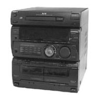
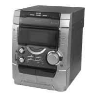
Related product manuals