91
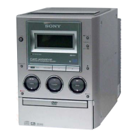
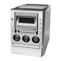
HCD-M90
Pin No. Pin Name I/O Description
51 XIFCS O
Chip select signal output to the system controller
52 VSS —
Ground terminal
53 X1 O
System clock output terminal (16.5 MHz)
54 X0 I
System clock input terminal (16.5 MHz)
55 VCC —
Power supply terminal (+3.3V)
56 CKSW1 I
Disc tray open/close detect switch input
57 OCSW1 I
Disc tray open/close detect switch input
58 CS0X O
Chip select signal output to the program ROM
59 CS1X —
Not used
60 CS2X O
Chip select signal output to the AV decoder
61 CS3X O
Chip select signal output to the AV decoder
62 CS4X O
Chip select signal output to the ARP
63 CS5X O
Chip select signal output to the servo DSP
64 C —
Capacitor connected terminal
65, 66 CS6X, CS7X O
Chip select signal output terminal Not used
67 XWAIT I
Wait signal input from the ARP and AV decoder
68 BGRNTX —
Not used
69 BGR —
Not used
70 XRD O
Read enable signal output
71 XWRH O
High byte write enable signal output
72 XWRL —
Not used
73 NMIX —
Not used
74 HSTX —
Not used
75 VSS —
Ground terminal
76 XFRRST I
Reset signal input from the system controller “L”: reset
77 CPUCK O
CPU clock signal output terminal Not used
78 OCSW2 —
Not used
79 XDACX —
Not used
80 VESCS/X39CS O
Chip select signal output to the audio DSP
81 48/44.1K O
Sampling frequency selection signal output terminal “L”: 48 kHz, “H”: 44.1 kHz
82 WIDE O
Wide signal output terminal Not used
83 MAMUTE I
System OK signal input from the system controller
84 XLDON O
LD control signal output ton the RF amp
85 to 100 HD0 to HD15 I/O
Two-way data bus
101 VSS —
Ground terminal
102 to 109 HA0 to HA7 O
Address signal output
110 VCC —
Power supply terminal (+3.3V)
111 to 118 HA8 to HA15 O
Address signal output
119 VSS —
Ground terminal
120 HA16 O
Address signal output
w
w
w
.
x
i
a
o
y
u
1
6
3
.
c
o
m
Q
Q
3
7
6
3
1
5
1
5
0
9
9
2
8
9
4
2
9
8
T
E
L
1
3
9
4
2
2
9
6
5
1
3
9
9
2
8
9
4
2
9
8
0
5
1
5
1
3
6
7
3
Q
Q
TEL 13942296513 QQ 376315150 892498299
TEL 13942296513 QQ 376315150 892498299
http://www.xiaoyu163.com
http://www.xiaoyu163.com