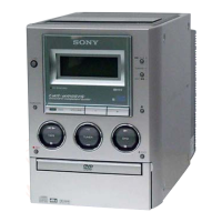
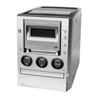
92
HCD-M90
• DVD BOARD IC302 CXD9635R (SERVO DIGITAL SIGNAL PROCESSOR, ARP)
Pin No. Pin Name I/O Description
1 VSS —
Ground terminal (for digital system)
2 to 9 D0 to D7 I/O
Two-way data bus
10 VDD 3.3V —
Power supply terminal (+3.3V) (for digital system)
11 to 15 A0 to A4 I
Address signal input from the DVD system controller
16 VSS —
Ground terminal (for digital system)
17 to 19 A5 to A7 I
Address signal input from the DVD system controller
20 VDD 1.8V —
Power supply terminal (+1.8V) (for digital system)
21 XINT O
Interrupt request signal output to the DVD system controller
22 HINT O
Interrupt request signal output to the DVD system controller
23 XCS I
Chip select signal input from the DVD system controller
24 HCS I
Chip select signal input from the DVD system controller
25 XWAT O
Wait signal output to the DVD system controller
26 VSS —
Ground terminal (for digital system)
27 to 36 MA0 to MA9 O
Address signal output to the D-RAM
37 VDD 3.3V —
Power supply terminal (+3.3V) (for digital system)
38 XMWR O
Write enable signal output to the D-RAM
39 XCAS O
CAS signal output to the D-RAM
40 VSS —
Ground terminal (for digital system)
41 XRAS O
RAS signal output to the D-RAM
42 XOE O
Output enable signal output to the D-RAM
43 VDD1 1.8V —
Power supply terminal (+1.8V) (for digital system)
44 to 51 MD0 to MD7 I/O
Two-way data bus with the D-RAM
52 VSS —
Ground terminal (for digital system)
53 to 60 MD8 to MD15 I/O
Two-way data bus with the D-RAM
61 VDD 3.3V —
Power supply terminal (+3.3V) (for digital system)
62 DATA O
CD data output to the AV decoder
63 BCLK O
CD bit clock signal output to the AV decoder
64 VSS —
Ground terminal (for digital system)
65 LRCK O
CD LR clock signal output to the AV decoder
66 DOUT O
Digital signal output to the AV decoder
67 VDD 1.8V —
Power supply terminal (+1.8V) (for digital system)
68 SDCK O
SD bus clock signal output to the AV decoder
69 XSHD O
SD bus header signal output to the AV decoder
70 XSRQ I
SD bus request signal input from the AV decoder
71 XSAK O
SD bus acknowledge signal output to the AV decoder
72 SDEF O
SD bus error flag signal output to the AV decoder
73 to 81 SD0 to SD7 O
SD bus data output to the AV decoder
82 VDD 3.3V —
Power supply terminal (+3.3V) (for digital system)
83 to 88 MNT0 to MNT5 I/O
Monitor signal input/output terminal Not used
89, 90 MNT6, MNT7 I/O
Monitor signal input/output terminal Not used
91 ESTB O
Error strobe signal output terminal Not used
92 VDD 1.8V —
Power supply terminal (+1.8V) (for digital system)
93 RFD I/O RF digital data input/output terminal Not used
94 VSS —
Ground terminal (for digital system)
w
w
w
.
x
i
a
o
y
u
1
6
3
.
c
o
m
Q
Q
3
7
6
3
1
5
1
5
0
9
9
2
8
9
4
2
9
8
T
E
L
1
3
9
4
2
2
9
6
5
1
3
9
9
2
8
9
4
2
9
8
0
5
1
5
1
3
6
7
3
Q
Q
TEL 13942296513 QQ 376315150 892498299
TEL 13942296513 QQ 376315150 892498299
http://www.xiaoyu163.com
http://www.xiaoyu163.com