93
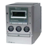
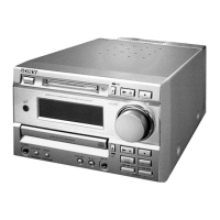
HCD-M90
Pin No. Pin Name I/O Description
95 PLCKO O
Not used
96 to 103 ADO0 to ADO7 O
Not used
104 VSS —
Ground terminal (for digital system)
105 VSSA4 —
Ground terminal (for analog system)
106 VCO I
VCO control signal input
107, 108 R1, R2 I
VCO outside resistance signal input
109 VDDA4 3.3V —
Power supply terminal (+3.3V) (for analog system)
110 VSSA3 —
Ground terminal (for analog system)
111 INP I
OP amp positive input terminal
112 INM I
OP amp negative input terminal
113 to 115 FR3 to FR1 I
Feedback resistance signal
116 Y O
OP amp output terminal
117 VDDA3 3.3V —
Power supply terminal (+3.3V) (for analog system)
118 VREF I
Reference voltage input terminal (for D/A converter)
119 BIAS I
Bias input terminal (for D/A converter)
120 VDDA2 3.3V —
Power supply terminal (+3.3V) (for analog system)
121 VSSA2 —
Ground terminal (for analog system)
122 AOUT O
D/A converter output terminal (for D/A converter)
123 IREF I
Reference current input terminal (for D/A converter)
124 VSSD2 —
Ground terminal (for D/A converter)
125 VDDD2 3.3V —
Power supply terminal (+3.3V) (for D/A converter)
126 VRT I
A/D converter reference input terminal
127 VDDA1 3.3V —
Power supply terminal (+3.3V) (for analog system)
128 RFIN2 I
RF signal input from the RF amp
129 NMIX —
RF signal input terminal Not used
130 VSSA1 —
Ground terminal (for analog system)
131 RFIN1 I
RF signal input from the RF amp
132 VRB I
A/D converter reference input terminal
133 VSSD1 —
Ground terminal (for A/D converter)
134 VDDD1 3.3V —
Power supply terminal (+3.3V) (for A/D converter)
135 ADC0 I
Tracking error signal input from the RF amp
136 ADC1 I
Focusing error signal input from the RF amp
137 ADC2 I
Pull-in signal input from the RF amp
138 VDDA0 3.3V —
Power supply terminal (+3.3V) (for analog system)
139 ADC3 I
Tracking coil drive signal input from the coil drive
140 ADC4 I
Spindle motor drive signal input from the motor drive
141 VSSA0 —
Ground terminal (for analog system)
142, 143 ADC5, ADC6 I
A/D converter input terminal
144 ADC7 I
Monitor signal input from the RF amp
145 VDDD0 3.3V —
Power supply terminal (+3.3V) (for A/D converter)
146 VSSD0 —
Ground terminal (for A/D converter)
147 VRBA I
A/D converter reference input terminal
148 VSSA0 —
Ground terminal (for analog system)
149 TESTAA O
ASW output terminal Not used
150 VDDA0 3.3V —
Power supply terminal (+3.3V) (for analog system)
w
w
w
.
x
i
a
o
y
u
1
6
3
.
c
o
m
Q
Q
3
7
6
3
1
5
1
5
0
9
9
2
8
9
4
2
9
8
T
E
L
1
3
9
4
2
2
9
6
5
1
3
9
9
2
8
9
4
2
9
8
0
5
1
5
1
3
6
7
3
Q
Q
TEL 13942296513 QQ 376315150 892498299
TEL 13942296513 QQ 376315150 892498299
http://www.xiaoyu163.com
http://www.xiaoyu163.com