94
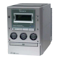
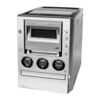
HCD-M90
Pin No. Pin Name I/O Description
151 VRTA I
A/D converter reference input terminal
152 VSS —
Ground terminal (for digital system)
153 to 155
TESTK0 to TESTK
I
Test signal input terminal (fixed at “L”)
156 XDSPRST I
DSP reset signal input from the DVD system controller “L”: reset
157 XARPRST I
ARP reset signal input from the DVD system controller “L”: reset
158 VSS —
Ground terminal (for digital system)
159 MDS0 O
Spindle motor drive signal output to the motor drive
160 MON O
Motor ON/OFF signal output terminal Not used
161 MDP0 O
Spindle motor drive signal output to the motor drive
162 DFCT O
Defect detection signal output
163 JITPWM O
Jitter PWM signal output terminal Not used
164 LOCK O
EFM lock detection signal output terminal Not used
165 VDD1 1.8V —
Power supply terminal (+1.8V) (for digital system)
166 GIO0/INT2 I
Inlimit sensor input terminal
167 GIO1/INT3 O
Spindle motor drive control signal output to the motor drive
168 GIO2/INT4 I
TSD-M signal input from the motor/coil drive
169 GIO3/INT5 —
Not used
170 VDD 3.3V —
Power supply terminal (+3.3V) (for digital system)
171 GIO4/PGREF —
Not used
172 GIO5/PGIN I
Monitor signal input from the RF amp
173 GIO6/SDI I
Serial data input from the RF amp
174 GIO7/SDO O
Serial data output to the RF amp
175 GIO8/SCK O
Serial clock signal output to the RF amp
176 GIO9/FGREF O
Loading motor drive signal output to the motor drive
177 GIO10/FGIN O
Loading motor drive signal output to the motor drive
178 GIO11/TMC2 —
Not used
179 GIO12 —
Not used
180 GIO13 O
Serial data enable signal output to the RF amp
181 VSS —
Ground terminal (for digital system)
182 CLKIN I
Clock signal input from the clock generator
183 VSSA5 —
Ground terminal (for analog system)
184 VDDA5 1.8V —
Power supply terminal (+1.8V) (for analog system)
185 DFCTI I
Defect signal input from the RF amp
186 VSS —
Ground terminal (for digital system)
187 MCKI I
Clock signal input from the clock generator
188 VDD 1.8V —
Power supply terminal (+1.8V) (for digital system)
189 SCKI I
Clock signal input from the clock generator
190 VSS —
Ground terminal (for digital system)
191 TRST I
Reset signal input terminal (for JTAG boundary scan)
192 TMS I
MS signal input terminal (for JTAG boundary scan)
193 TDI I
Serial data input terminal (for JTAG boundary scan)
194 TCK I
Clock signal input terminal (for JTAG boundary scan)
195 TDO O
Serial data output terminal (for JTAG boundary scan)
196 TZC I
Tracking zero crossing signal input from the RF amp
197 MIRR I
Mirror detect signal input terminal from the RF amp
w
w
w
.
x
i
a
o
y
u
1
6
3
.
c
o
m
Q
Q
3
7
6
3
1
5
1
5
0
9
9
2
8
9
4
2
9
8
T
E
L
1
3
9
4
2
2
9
6
5
1
3
9
9
2
8
9
4
2
9
8
0
5
1
5
1
3
6
7
3
Q
Q
TEL 13942296513 QQ 376315150 892498299
TEL 13942296513 QQ 376315150 892498299
http://www.xiaoyu163.com
http://www.xiaoyu163.com