Table 22 describes the connections of the USB Type-C
®
connector (CN4).
Table 22. USB Type-C
®
receptacle connector (CN4)
Pin
number
Description Signal assignment
Pin
number
Description Signal assignment
B12 GND GND A1 GND GND
B11 RX1_P - A2 TX1_P -
B10 RX1_N - A3 TX1_N -
B9 VBUS VBUSc A4 VBUS VBUSc
B8 SBU2 - A5
CC1
(1)
CC1c
B7 DM2 USBC_CN_HS_N (PA11) A6 DP1 USBC_CN_HS_P (PA12)
B6 DP2 USBC_CN_HS_P (PA12) A7 DM1 USBC_CN_HS_N (PA11)
B5
CC2
(1)
CC2c A8 SBU1 -
B4 VBUS VBUSc A9 VBUS VBUSc
B3 TX2_N - A10 RX2_N -
B2 TX2_P - A11 RX2_P -
B1 GND GND A12 GND GND
1. By default, the CCx signals from CN4 are connected to the CCxc pins of TCPP01-M12. Depending on use cases, CCx
signals might be used to connect to UCPD.ADCx signals of MCU (PG0 and PF15)
13.2
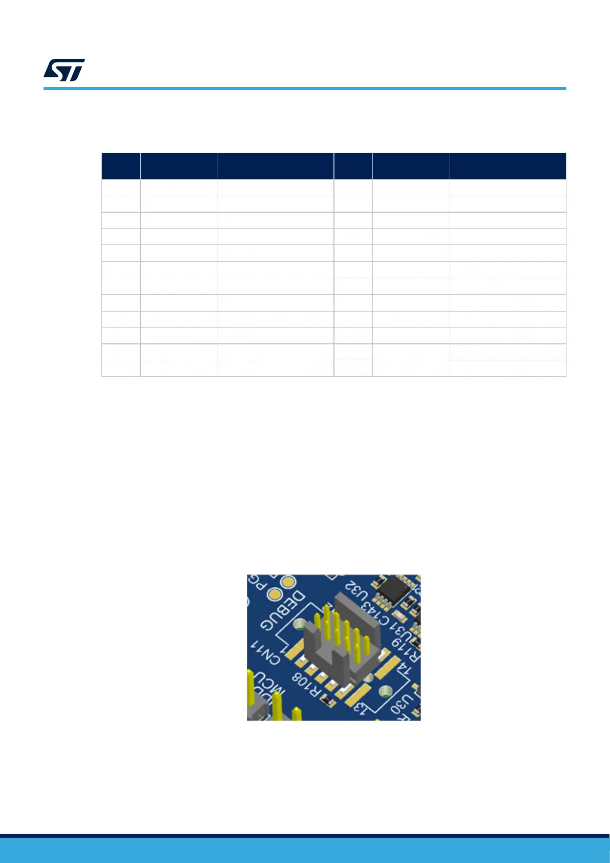
Debug connector (CN11)
The Discovery kit embeds a MIPI10 debug connector on the bottom side of the main board (the 14-pin footprint
also enables the support of an STDC14 connector as an option):
• MIPI10 10-pin connector on the 14‑pin footprint (default configuration)
• STDC14 14‑pin connector (option)
Attention: Before using CN11, check specific constraints in Section 12.14 SWD debug/program/trace and JTAG/USART.
13.2.1 MIPI10 debug connector (default configuration)
Figure 25. MIPI10 debug connector (CN11)
UM2967
Debug connector (CN11)
UM2967 - Rev 1
page 40/68