Function GPIO Signal name Pin number (CN2) Signal name GPIO Function
- - NC 39 40 I2C5.SDA PH4
Touch panel I2C
data
- - NC 41 42 NC - -
SWIRE PI7 DSI_SWIRE 43 44 I2C5.SCL PH5
Touch panel I2C
clock
- - NC 45 46 NC - -
- - NC 47 48 NC - -
Tearing effect PF11 DSI_TE 49 50 NC - -
- - NC 51 52 NC - -
DSI Backlight
control output
PI6 DSI_BL_CTRL 53 54 NC - -
- - NC 55 56 NC - -
DSI and touch
panel reset output
PD5 DSI_RESETn 57 58 NC - -
- - NC 59 60 1V8_LCD - 1.8V voltage
General ground - GND 61 62 GND - General ground
General ground - GND 63 64 GND - General ground
1. The microcontroller software system must invert DSI.CK_N and DSI.CK_P lines together to be aligned with the DSI_V3
add
‑
on boards. The DSI clock differential signals (_N and _P) are originally inverted on the main board for layout reasons
(refer to DSI_V3 connector standard pinning).
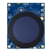
13.5
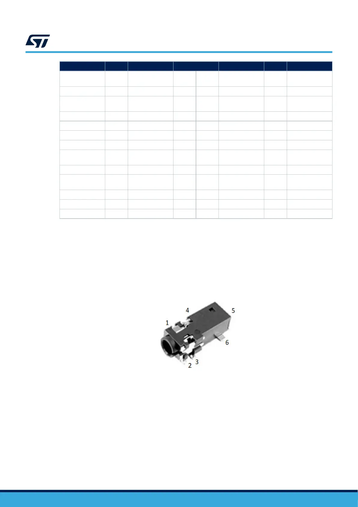
Audio jack (not used) (CN6)
Note: SAI audio codec and audio jack are not present by default.
The 3.5 mm stereo audio jack supports stereo line or headphone outputs and an analog microphone:
Figure 30. Audio jack connector (CN6)
UM2967
Audio jack (not used) (CN6)
UM2967 - Rev 1
page 44/68