User manual 5-2
DSC/DSCT Series
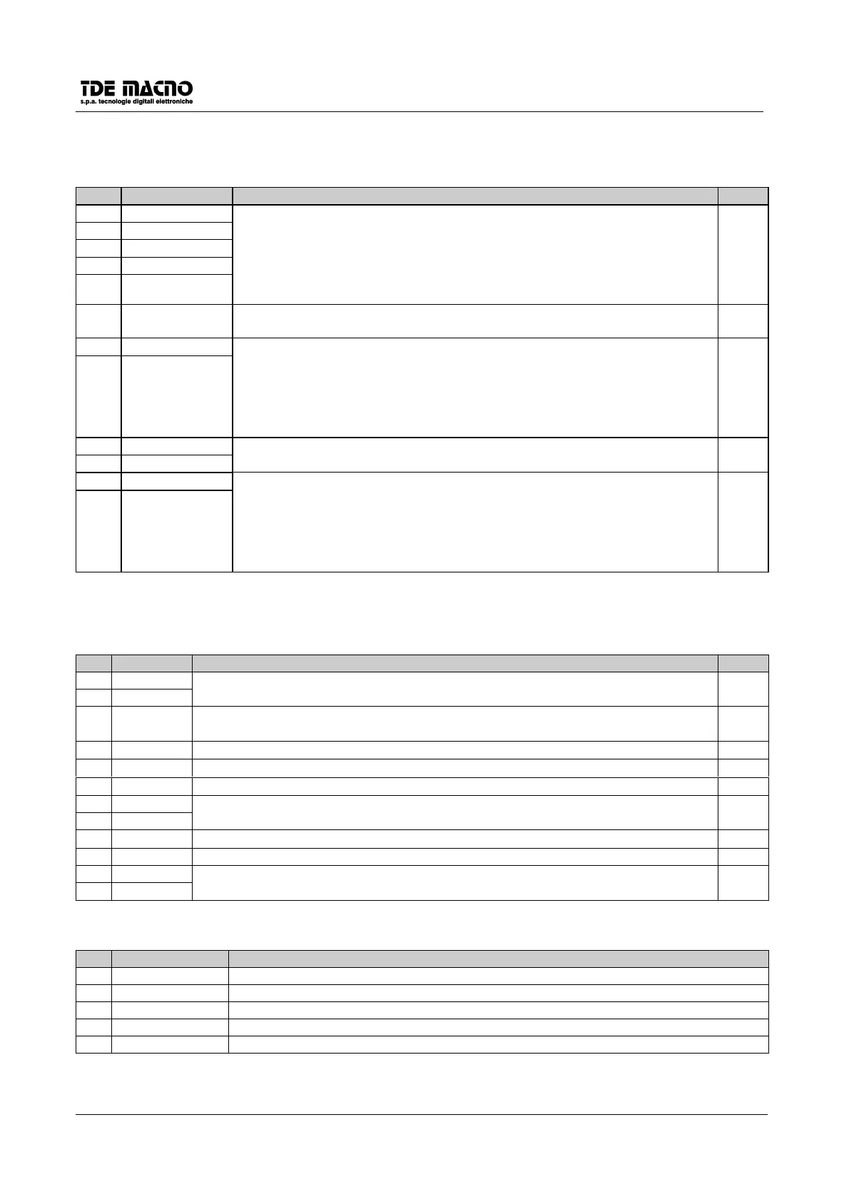
5.3. SIGNALS ON THE CONNECTORS
5.3.1. LOGIC SIGNALS (CONNECTOR J1)
PIN FUNCTION DESCRIPTION PAR.
1 L.I.1
2 L.I.2
3 L.I.3
4 L.I.4
5 L.I.5
Logic configurable inputs
ON = +24Vdc (>18Vcc) 10mA max.
OFF = 0Vcc (<6Vcc)
All inputs are opto-insulated from the internal regulation.
7.1
6 L.I.C Common connection of the logic inputs. Connect to the negative pole of the
inputs supply.
7.1
7 L.O.1
8/L.O.1
Logic configurable output
Transistor NPN with free collector ( L.O.1 ) and emitter ( /L.O.1 ), insulated
from the regulation and protected from overvoltage.
In CONDUCTION when output is ACTIVE : +24 Vdc 30 mA max;
7.2
90VP
10 +24V
Internal supply +24V, insulated from the regulation
11 L.O.2
12 /L.O.2
Logic configurable output
Transistor NPN with free collector ( L.O.1 ) and emitter ( /L.O.1 ), insulated
from the regulation and protected from overvoltage.
In CONDUCTION when output is ACTIVE : +24 Vdc 30 mA max;
7.2
5.3.2. ANALOG SIGNALS (CONNECTOR J2)
PIN
FUNCTION
PAR.
10V
20V
Regulation 0V
3 A.P.O.
Analog configurable output: ±10V /2mA
Default configuration: CURRENT REQUEST(c13=11)
7.3
4 I.OUT
Current request output signal ±10V <2mA
5TG.O
Motor speed analog output ±10V <2mA
6 I.LIM
Analog input Max. Current Limit 0÷+10V <0.5mA
7+10V
80V
+10V / 10mA max.
Stabilized power supply
9T.REF
Analog input Torque Reference ±10V <0.5mA
10 0V 0V of the speed reference
11 S.REF Speed reference differential input.
12 /S.REF
±2.5V÷ ±10V <0.5mA
5.3.3. FREQUENCY INPUT CONNECTOR (CONNECTOR J6)
PIN FUNCTION
1 FA Channel /A input.
2 FA/ (F) Channel A/ input or frequency input.
3 FB Channel B input.
4 FA (UP/DOWN) Channel B/ input or UP/DOWN
5 0DG 0V of the frequency input
 Loading...