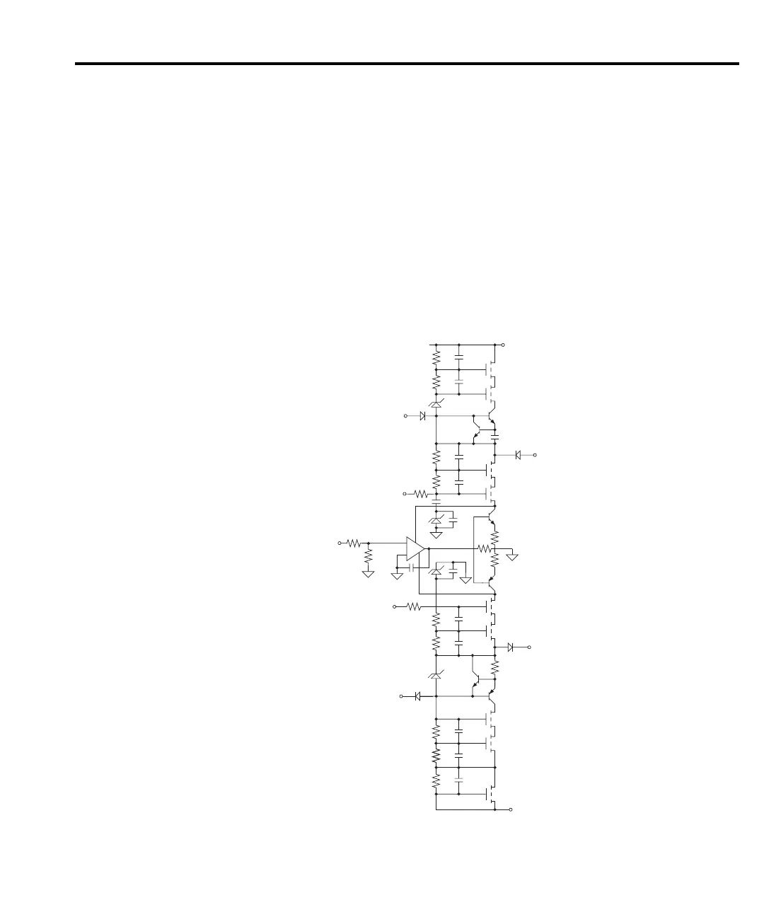
Output stage
Figure
4-4 shows a simplified schematic of the output stage.
The Model 2410 output stage serves two purposes: (1) it converts signals from floating
common to output common, and (2) it provides both voltage and current amplification. The
output stage drive transistors are biased in class B configuration to prevent the possibility of
thermal runaway with high-current output values. High-current taps for the ±20V outputs are
provided to reduce power dissipation on the 20V and lower ranges.
Output transistors Q518 and Q521 are cascoded with output MOSFETs Q516 and Q523. All
o
t
her MOSFETs and transistors are slaves, and the voltages across these devices are determined
by the resistor-capacitor ladder circuits shown. Coarse current limits are built into the output
stage.
Figure 4-4
Output stage
simplified
schematic
Troubleshooting 4-9
F
O
+
-
F
F
F
+1200V
Q500
Q502
Q504
Q505
+42V
Q514
Q516
Q518
+Hi Drive
Maindrive
300K
Q521
-30VF
Q523
Q525
-42V
Q506
Q507
Q509
Q533
Q511
-1200V
-Hi Drive
+15VF
2410-902-01.book Page 9 Monday, November 7, 2005 2:49 PM