www.ti.com
I
2
C Registers
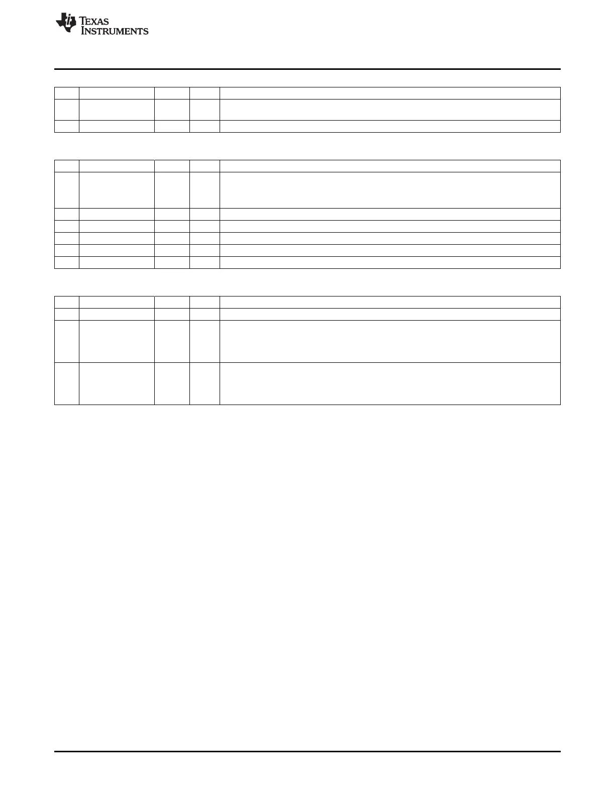
I2CADDR (0x6233) – I
2
C Own Slave Address
Bit Name Reset R/W Description
7:1
ADDR
0000 00 R/W Own slave address
0
0
GC
0 R/W General-call address acknowledge. If set, the general-call address is recognized.
I2CWC (0x6234) – Wrapper control
Bit Name Reset R/W Description
7
OVR
0 R/W Override enable:
0: I
2
C functionality (ignore other bits in this register)
1: GPIO functionality.-
6:4 – 000 R0 Reserved
3
SCLPUE
1 R/W SCL pin pullup enable
2
SDAPUE
1 R/W SDA pin pullup enable
1
SCLOE
0 R/W SCL pin output enable
0
SDAOE
0 R/W SDA pin output enable
I2CIO (0x6235) – GPIO
Bit Name Reset R/W Description
7:2 – 000 R0 Reserved
1
SCLD
0 R/W SCL data value
When I2CWC.SCLOE is set, reading SCLD reads the output register, not the pin. When
I2CWC.SCLOE is cleared, reading SCLD reads the pin. Writing SCLD writes to the output
register.
0
SDAD
0 R/W SDA data value
When I2CWC.SDAOE is set, reading SDAD reads the output register, not the pin. When
I2CWC.SDAOE is cleared, reading SDAD reads the pin. Writing SDAD writes to the output
register.
189
SWRU191C–April 2009–Revised January 2012
I
2
C
Submit Documentation Feedback
Copyright © 2009–2012, Texas Instruments Incorporated
 Loading...


