Memory
www.ti.com
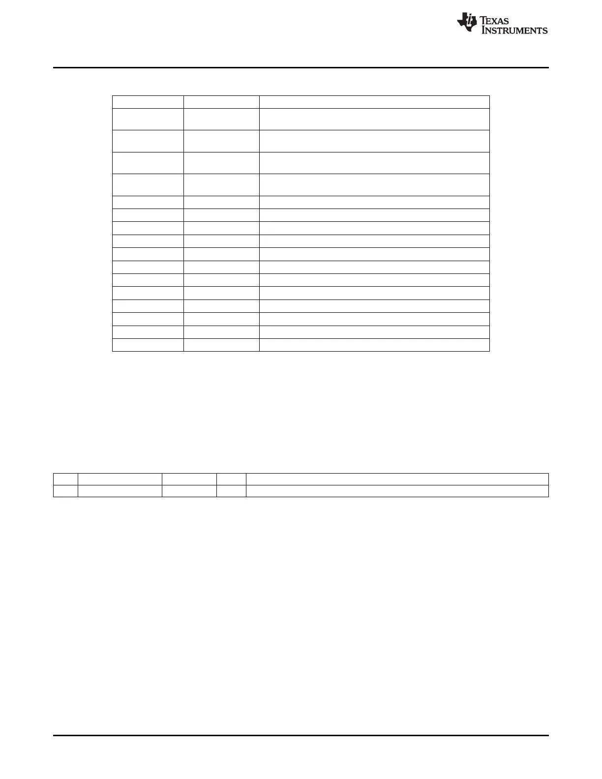
Table 2-2. Overview of XREG Registers (continued)
XDATA Address Register Name Description
Timer 1 channel 1 capture/compare value low (additional XREG
0x62A8 T1CC1L
mapping of SFR register)
Timer 1 channel 1 capture/compare value high (additional
0x62A9 T1CC1H
XREG mapping of SFR register)
Timer 1 channel 2 capture/compare value low (additional XREG
0x62AA T1CC2L
mapping of SFR register)
Timer 1 channel 2 capture/compare value high (additional
0x62AB T1CC2H
XREG mapping of SFR register)
0x62AC T1CC3L Timer 1 channel 3 capture/compare value low
0x62AD T1CC3H Timer 1 channel 3 capture/compare value high
0x62AE T1CC4L Timer 1 channel 4 capture/compare value low
0x62AF T1CC4H Timer 1 channel 4 capture/compare value high
0x62B0 STCC Sleep Timer capture control
0x62B1 STCS Sleep Timer capture status
0x62B2 STCV0 Sleep Timer capture value byte 0
0x62B3 STCV1 Sleep Timer capture value byte 1
0x62B4 STCV2 Sleep Timer capture value byte 2
0x62C0 OPAMPC Operational amplifier control
0x62C1 OPAMPS Operational amplifier status
0x62D0 CMPCTL Analog comparator control and status
2.2.4 XDATA Memory Access
The MPAGE register is used during instructions MOVX A,@Ri and MOVX @Ri,A. MPAGE gives the 8
most-significant address bits, whereas the register Ri gives the 8 least-significant bits.
In some 8051 implementations, this type of XDATA access is performed using P2 to give the
most-significant address bits. Existing software may therefore have to be adapted to make use of MPAGE
instead of P2.
MPAGE (0x93) – Memory Page Select
Bit Name Reset R/W Description
7:0
MPAGE[7:0]
0x00 R/W Memory page, high-order bits of address in MOVX instruction
2.2.5 Memory Arbiter
The memory arbiter handles CPU and DMA access to all physical memory except the CPU internal
registers. When an access conflict between the CPU and DMA occurs, the memory arbiter stalls one of
the bus masters so that the conflict is resolved.
The control registers MEMCTR and FMAP are used to control various aspects of the memory subsystem.
The MEMCTR and FMAP registers are described as follows.
MEMCTR.XMAP must be set to enable program execution from RAM.
The flash-bank map register, FMAP, controls mapping of physical 32-KB code banks to the program
address region 0x8000–0xFFFF in CODE memory space.
36
8051 CPU SWRU191C–April 2009–Revised January 2012
Submit Documentation Feedback
Copyright © 2009–2012, Texas Instruments Incorporated
 Loading...


