0 xFFFF
0x8000
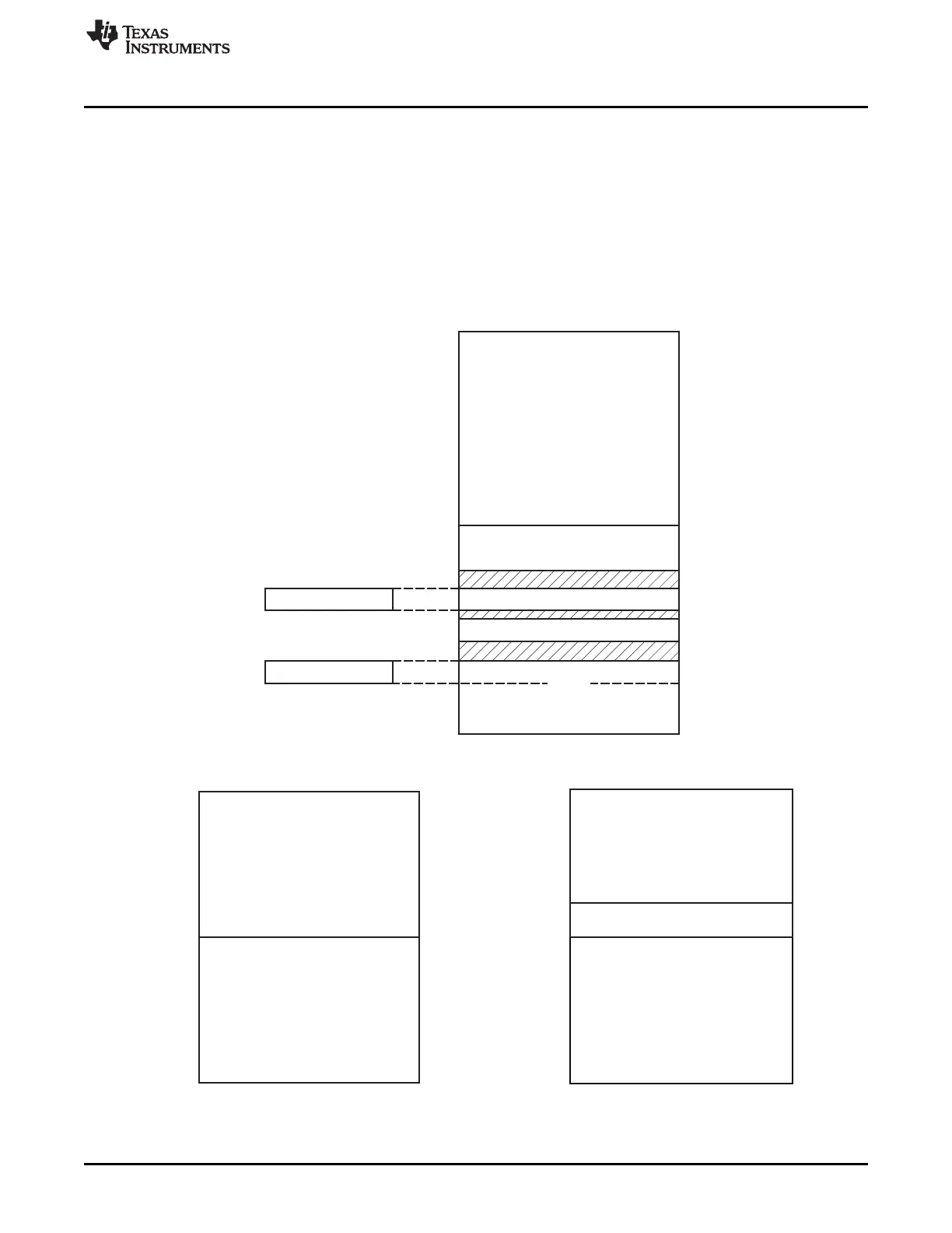
0x0000
0x 6000
XREG(1KB)
0x63FF
SFR(128B)
0x 7080
SRAM_SIZE – 1
SRAMSIZE – 256
0x7 FFF
XBANK
(SELECTABLE32KBFLASHBANK)
8051SFRSPACE
8051DATA SPACE
INFORMATIONPAGE
(2KB)
0x70FF
0x 7800
M0097-02
SRAM
(SRAM_SIZEBytes)
0x 0000
0x7FFF
0x 8000
0 xFFFF
Bank0–7
(32KBFLASH)
Common Area/Bank0
(32KBFLASH)
M0098-02
0x 0000
0x7FFF
0x 8000
0 xFFFF
SRAM
0x8000 + SRAM_SIZE – 1
0x8000 + SRAM_SIZE
Banks 0–7
(Upper 24KB FLASH)
Common Area/Bank 0
(32KB FLASH)
M0099-04
www.ti.com
Memory
The second scheme is used for executing code from SRAM. In this mode, the SRAM is mapped into the
region of 0x8000 through (0x8000 + SRAM_SIZE – 1). The map is shown in Figure 2-2. Executing code
from SRAM improves performance and reduces power consumption.
The upper 32 KB of XDATA is a read-only area called XBANK. Any of the available 32 KB flash banks can
be mapped in here. This gives software access to the whole flash memory. This area is typically used to
store additional constant data.
Details about mapping of all 8051 memory spaces are given in Section 2.2.2.
The memory map showing how the different physical memories are mapped into the CPU memory spaces
is given in Figure 2-1 through Figure 2-3. The number of available flash banks depends on the flash size
option.
Figure 2-1. XDATA Memory Space (Showing SFR and DATA Mapping)
Figure 2-2. CODE Memory Space Figure 2-3. CODE Memory Space for Running Code
From SRAM
29
SWRU191C–April 2009–Revised January 2012 8051 CPU
Submit Documentation Feedback
Copyright © 2009–2012, Texas Instruments Incorporated
 Loading...


