Registers
www.ti.com
To set up the packet-sniffer signals or some of the other RF core observation outputs (in total maximum 3;
rfc_obs_sig0, rfc_obs_sig1, and rfc_obs_sig2), the user must perform the following steps:
Step1: Determine which signal (RFC_OBS_CTRL[0–2]) to output on which GPIO pin (P1[0:5]). This is
done using the OBSSELx control registers (OBSSEL0–OBSSEL5) that control the observation output to the
pins P1[0:5] (overriding the standard GPIO behavior for those pins).
Step2: Set the (RFC_OBS_CTRL[0–2]) control registers to select the correct signals (rfc_obs_sig); e.g.,
for packet sniffing one needs the rfc_sniff_data for the packet-sniffer data signal.and rfc_sniff_clk for the
corresponding clock signal.
Step3: Enable the packet-sniffer module in the MDMCTRL3 register.
25.12 Registers
25.12.1 Register Overview
25.12.1.1 SFR Registers
1 - RFIRQF0 (0xE9) RF interrupt flags
2 - RFIRQF1 (0x91) RF interrupt flags
3 - RFERRF (0xBF) RF error interrupt flags
4 - RFD (0xD9) RF data
5 - RFST (0x6189) LLE and FIFO commands
25.12.1.2 XREG Registers
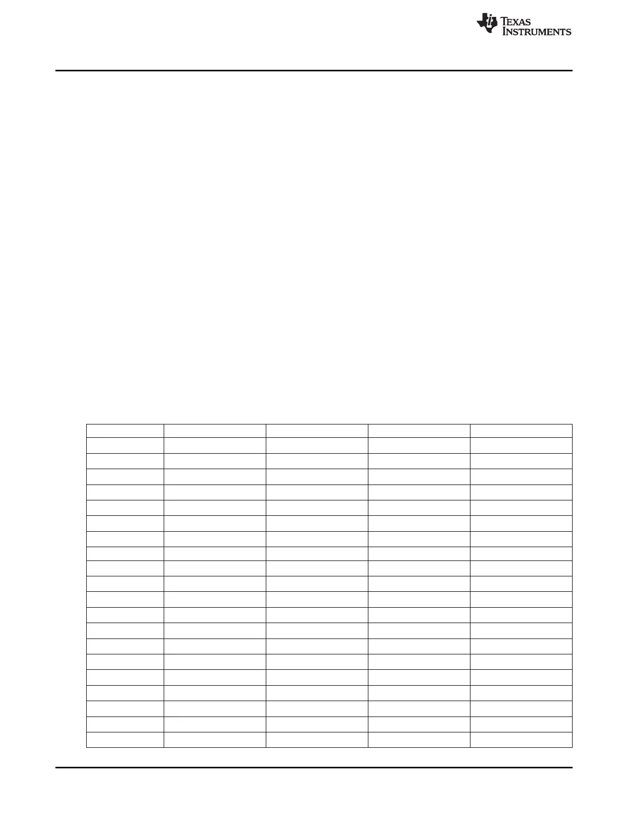
Table 25-23. XREG Register Overview
Address (Hex) + 0x0000 + 0x001 + 0x002 + 0x003
0x6180
FRMCTRL0 RFIRQM0 RFIRQM1 RFERRM
0x6184
FREQCTRL FREQTUNE TXPOWER TXCTRL
0x6188
LLESTAT SEMAPHORE0 SEMAPHORE1
0x618C
SEMAPHORE2 RFSTAT RSSI RFPSRND
0x6190
MDMCTRL0 MDMCTRL1 MDMCTRL2 MDMCTRL3
0x6194
SW_CONF SW0 SW1 SW2
0x6198
SW3 FREQEST RXCTRL FSCTRL
0x619C
0x61A0
LNAGAIN AAFGAIN ADCTEST0
0x61A4
MDMTEST0 MDMTEST1
0x61A8
ATEST
0x61AC
RFC_OBS_CTRL0 RFC_OBS_CTRL1
0x61B0
RFC_OBS_CTRL2 LLECTRL
0x61BC
TXFILTCFG RFRND
0x61C0
RFRAMCFG RFFDMA0
0x61C4
RFFDMA1 RFFSTATUS RFFCFG
0x61C8
RFRXFLEN RFRXFTHRS RFRXFWR RFRXFRD
0x61CC
RFRXFWP RFRXFRP RFRXFSWP RFRXFSRP
0x61D0
RFTXFLEN RFTXFTHRS RFTXFWR RFTXFRD
0x61D4
RFTXFWP RFTXFRP RFTXFSWP RFTXFSRP
332
CC2541 Proprietary Mode Radio SWRU191C–April 2009–Revised January 2012
Submit Documentation Feedback
Copyright © 2009–2012, Texas Instruments Incorporated
 Loading...


