7 Series FPGAs GTP Transceivers User Guide www.xilinx.com 65
UG482 (v1.9) December 19, 2016
Loopback
Loopback testing can be used either during development or in deployed equipment for fault
isolation. The traffic patterns used can be either application traffic patterns or specialized
pseudo-random bit sequences. Each GTP transceiver has a built-in PRBS generator and checker.
Each GTP transceiver features several loopback modes to facilitate testing:
• Near-end PCS Loopback (path 1 in Figure 2-22)
The RX elastic buffer must be enabled and RX_XCLK_SEL must be set to RXREC for
Near-end PCS loopback to function properly.
While in Near-end PCS loopback, the RX XCLK domain is clocked by the TX PMA parallel
clock (TX XCLK). If the RXOUTCLK is used to clock FPGA logic and RXOUTCLKSEL is
set to RXOUTCLKPMA during normal operation, one of the following two items must be
changed when placing the GTP transceiver into Near-end PCS Loopback.
1.) Set RXOUTCLKSEL to select RXOUTCLKPCS
or
2.)Set RXCDRHOLD = 1'b1
• Near-end PMA Loopback (path 2 in Figure 2-22)
A GTRXRESET is required after entering and exiting Near-end PMA loopback.
• Far-end PMA Loopback (path 3 in Figure 2-22)
The TX buffer must be enabled and TX_XCLK_SEL must be set to TXOUT for Far-end PMA
loopback to function properly.
While in Far-end PMA loopback, the write side of the TX buffer is clocked by the RX PMA
parallel clock (RX XCLK).
A GTTXRESET is required after entering and exiting Far-end PMA loopback.
• Far-end PCS Loopback (path 4 in Figure 2-22)
If clock correction is not used, a transceiver in Far-end PCS loopback must use the same
reference clock used by the transceiver that is the source of the loopback data. Regardless of
whether clock correction is used or not, the ports TXUSRCLK and RXUSRCLK must be
driven by the same clocking resource (BUFG, BUFH).
Far-end PCS loopback is not supported when both or either gearbox in the channel is enabled.
Ports and Attributes
Table 2-27 and Table 2-28 define the loopback ports and attributes, respectively.
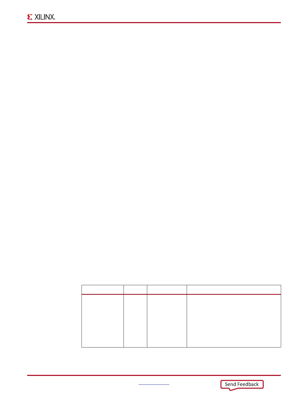
Table 2-27: Loopback Ports
Port Dir Clock Domain Description
LOOPBACK[2:0] In Async 000: Normal operation
001: Near-End PCS Loopback
010: Near-End PMA Loopback
011: Reserved
100: Far-End PMA Loopback
101: Reserved
110: Far-End PCS Loopback