146 www.xilinx.com 7 Series FPGAs GTP Transceivers User Guide
UG482 (v1.9) December 19, 2016
Chapter 4: Receiver
RX Fabric Clock Output Control
Functional Description
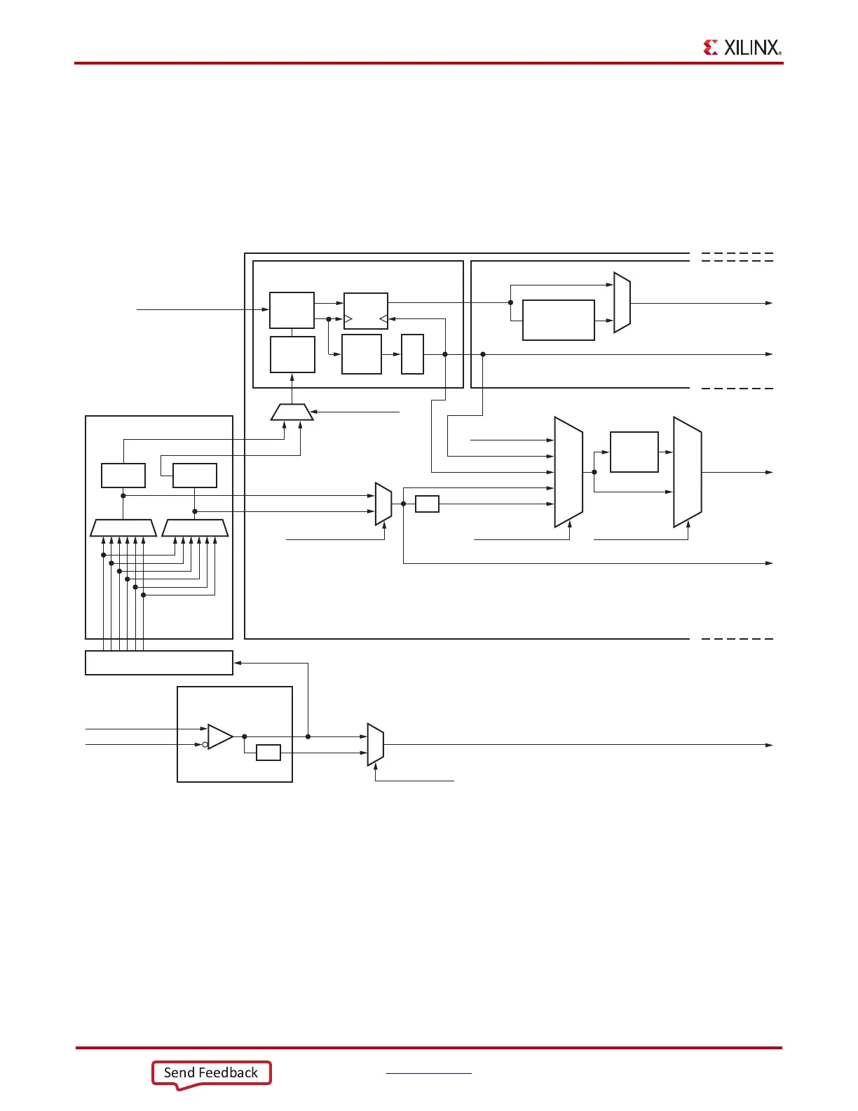
The RX clock divider control block has two main components: serial clock divider control and
parallel clock divider and selector control. The clock divider and selector details are illustrated in
Figure 4-18.
Note relevant to Figure 4-18:
1. RXOUTCLKPCS and RXOUTCLKFABRIC are redundant outputs. RXOUTCLK should be
used for new designs.
2. The REFCLK_CTRL option is controlled automatically by software and is not user selectable.
The user can only route one of IBUFDS_GTE2’s O or ODIV2 outputs to the FPGA logic.
3. IBUFDS_GTE2 is a redundant output for additional clocking scheme flexibility.
4. The selection of the /4 or /5 divider block is controlled by the RX_DATA_WIDTH attribute
from the GTPE2_CHANNEL primitive. /4 is selected when RX_DATA_WIDTH = 16 or 32. /5
is selected when RX_DATA_WIDTH = 20 or 40.
X-Ref Target - Figure 4-18
Figure 4-18: RX Serial and Parallel Clock Divider
UG482_C4_10_021113
PLL0
GTPE2_
COMMON
GTPE2_CHANNEL (GTP Transceiver Primitive)
IBUFDS_GTE2
RX PMA
RX PCS
REFCLK Distribution
PLL1
/D
{1,2,4,8}
SIPO
/2
/2
Delay
Aligner
PLL1OUTCLK
‘1’
RXOUTCLKPCS
RXOUTCLKPMA
PLL0REFCLK
PLL1REFCLK
O
ODIV2
RXOUTCLK
RXOUTCLKPCS
1
RXDATA to
Downstream
PCS Blocks
RXPLLREFCLK_DIV1
RXPLLREFCLK_DIV2
RXOUTCLKFABRIC
1
IBUFDS_GTE2 Output to Logic
3
RXOUTCLKSELRXSYSCLKSEL[1]
REFCLK_CTRL
2
RXSYSCLKSEL[0]
RXDLYBYPASS
000
001
0
1
010
011
100
PLL0OUTCLK
1
0
1
0
1
0
/4 or
/5
/2
RXP/N
RXDATA
RX Polarity
Control
MGTREFCLK[0/1]P
MGTREFCLK[0/1]N
REFCLK Sel REFCLK Sel
CDR