240 www.xilinx.com 7 Series FPGAs GTP Transceivers User Guide
UG482 (v1.9) December 19, 2016
Appendix A: Placement Information by Package
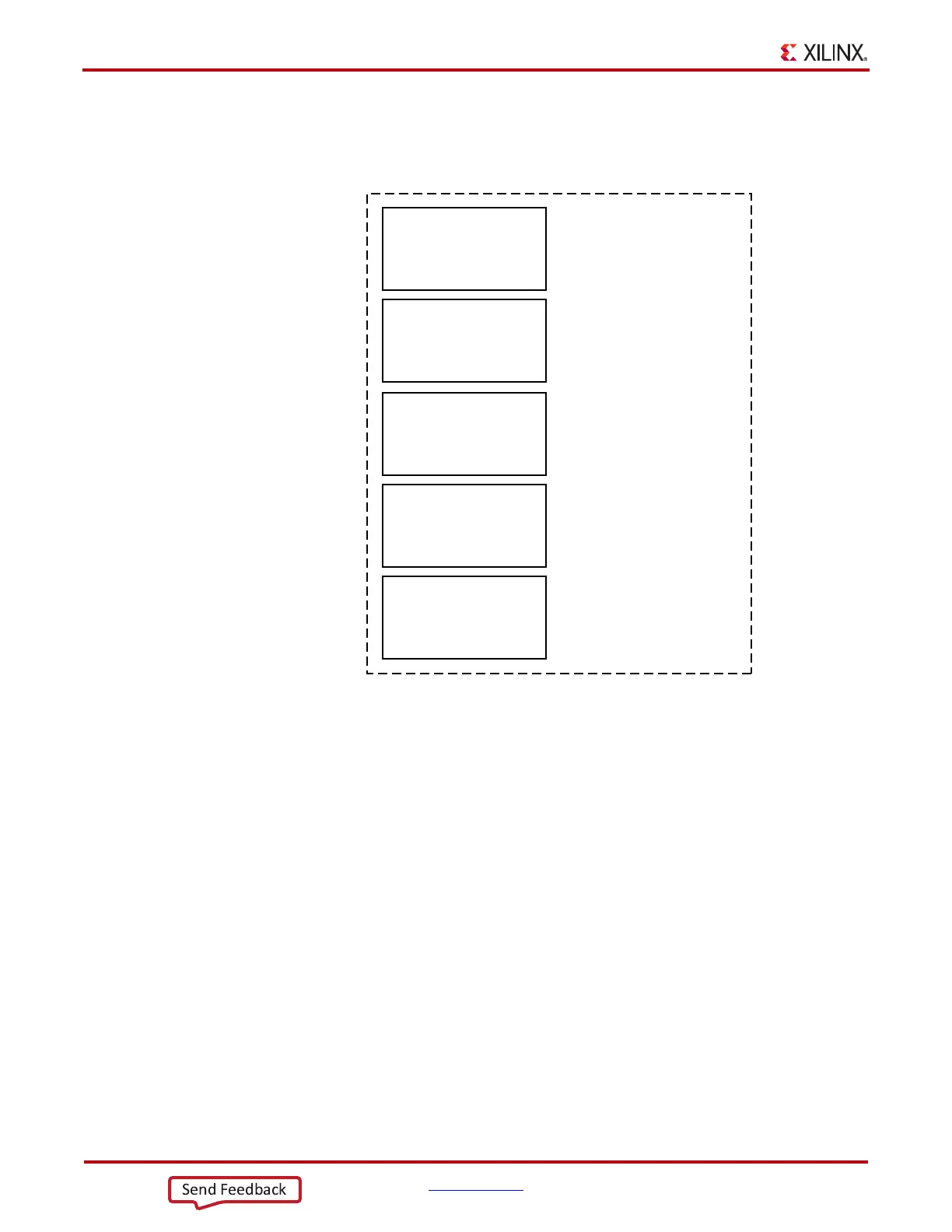
CLG485 Package Placement Diagram
Figure A-3 and shows the placement diagram for the CLG485 package.
X-Ref Target - Figure A-3
Figure A-3: Placement Diagram for the CLG485 Package
W2 MGTPTXP3_112
Y2 MGTPTXN3_112
W6 MGTPRXP3_112
Y6 MGTPRXN3_112
AA5 MGTPTXP2_112
UG482_aA_12_121916
AB5 MGTPTXN2_112
AA9 MGTPRXP2_112
AB9 MGTPRXN2_112
U5 MGTREFCLK1P_112
V5 MGTREFCLK1N_112
V9 MGTREFCLK0P_112
U9 MGTREFCLK0N_112
W4 MGTPTXP1_112
Y4 MGTPTXN1_112
W8 MGTPRXP1_112
Y8 MGTPRXN1_112
AA3 MGTPTXP0_112
AB3 MGTPTXN0_112
AA7 MGTPRXP0_112
AB7 MGTPRXN0_112
XC7Z012S:
GTPE2_CHANNEL_X0Y3
XC7Z015:
GTPE2_CHANNEL_X0Y3
XC7Z012S:
GTPE2_CHANNEL_X0Y2
XC7Z015:
GTPE2_CHANNEL_X0Y2
XC7Z012S:
GTPE2_COMMON_X0Y0
XC7Z015:
GTPE2_COMMON_X0Y0
XC7Z012S:
GTPE2_CHANNEL_X0Y1
XC7Z015:
GTPE2_CHANNEL_X0Y1
XC7Z012S:
GTPE2_CHANNEL_X0Y0
XC7Z015:
GTPE2_CHANNEL_X0Y0