7 Series FPGAs GTP Transceivers User Guide www.xilinx.com 125
UG482 (v1.9) December 19, 2016
Chapter 4
Receiver
RX Overview
Functional Description
This section shows how to configure and use each of the functional blocks inside the receiver (RX).
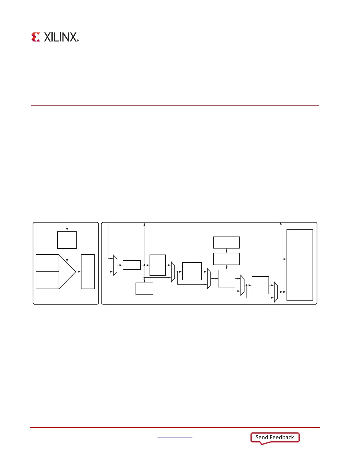
Each GTP transceiver includes an independent receiver, made up of a PCS and a PMA. Figure 4-1
shows the blocks of the GTP transceiver RX. High-speed serial data flows from traces on the board
into the PMA of the GTP transceiver RX, into the PCS, and finally into the FPGA logic. Refer to
Figure 2-9, page 35 for the description of the channel clocking architecture, which provides clocks
to the RX and TX clock dividers.
The key elements within the GTP transceiver RX are:
1. RX Analog Front End, page 126
2. RX Out-of-Band Signaling, page 131
3. RX Equalizer, page 139
4. RX CDR, page 141
5. RX Fabric Clock Output Control, page 147
6. RX Margin Analysis, page 151
7. RX Polarity Control, page 158
8. RX Pattern Checker, page 159
X-Ref Target - Figure 4-1
Figure 4-1: GTP Transceiver RX Block Diagram
Clock from
PLL0 or PLL1
From TX Parallel
Data (Near-End
PCS Loopback)
To TX Parallel
Data (Far-End
PMA Loopback)
To TX Parallel
Data (Far-End PCS
Loopback)
RX EQ
RX
Clock
Dividers
SIPO
RX OOB
Polarity
PRBS
Checker
Comma
Detect
and
Align
RX
Gearbox
FPGA RX
Interface
8B/10B
Decoder
RX
Elastic
Buffer
RX PIPE
Control
RX Status
Control
UG482_c4_01_110911