224 www.xilinx.com 7 Series FPGAs GTP Transceivers User Guide
UG482 (v1.9) December 19, 2016
Chapter 5: Board Design Guidelines
Reference Clock
Overview
This section focuses on the selection of the reference clock source or oscillator. An oscillator is
characterized by:
• Frequency range
• Output voltage swing
• Jitter (deterministic, random, peak-to-peak)
• Rise and fall times
• Supply voltage and current
• Noise specification
• Duty cycle and duty-cycle tolerance
• Frequency stability
These characteristics are selection criteria when choosing an oscillator for a GTP transceiver design.
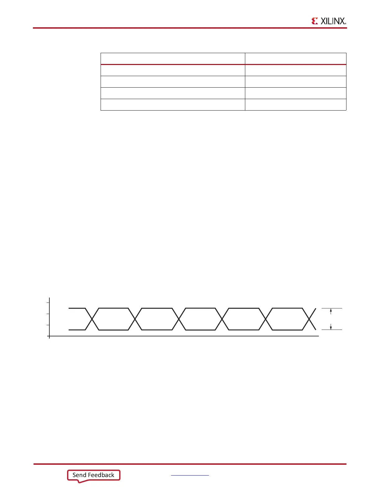
Figure 5-4 illustrates the convention for a single-ended clock input voltage swing, peak-to-peak.
This figure is provided to show the contrast to the differential clock input voltage swing calculation
shown in Figure 5-5.
MGTREFCLKP/MGTREFCLKN Float (if not used)
MGTRXP/MGTRXN GND
MGTTXP/MGTTXN Float
MGTRREF MGTAVTT through a 100Ω resistor
Table 5-6: Unused GTP Quad Column Connections (Cont’d)
Pin or Pin Pair of the Unused GTP Quad Connection
X-Ref Target - Figure 5-4
Figure 5-4: Single-Ended Clock Input Voltage Swing, Peak-to-Peak
MGTREFCLKP
UG482_c5_04_080612
Single-ended
Voltage
MGTREFCLKN
+V
0