7 Series FPGAs GTP Transceivers User Guide www.xilinx.com 93
UG482 (v1.9) December 19, 2016
TX Buffer
TX Buffer
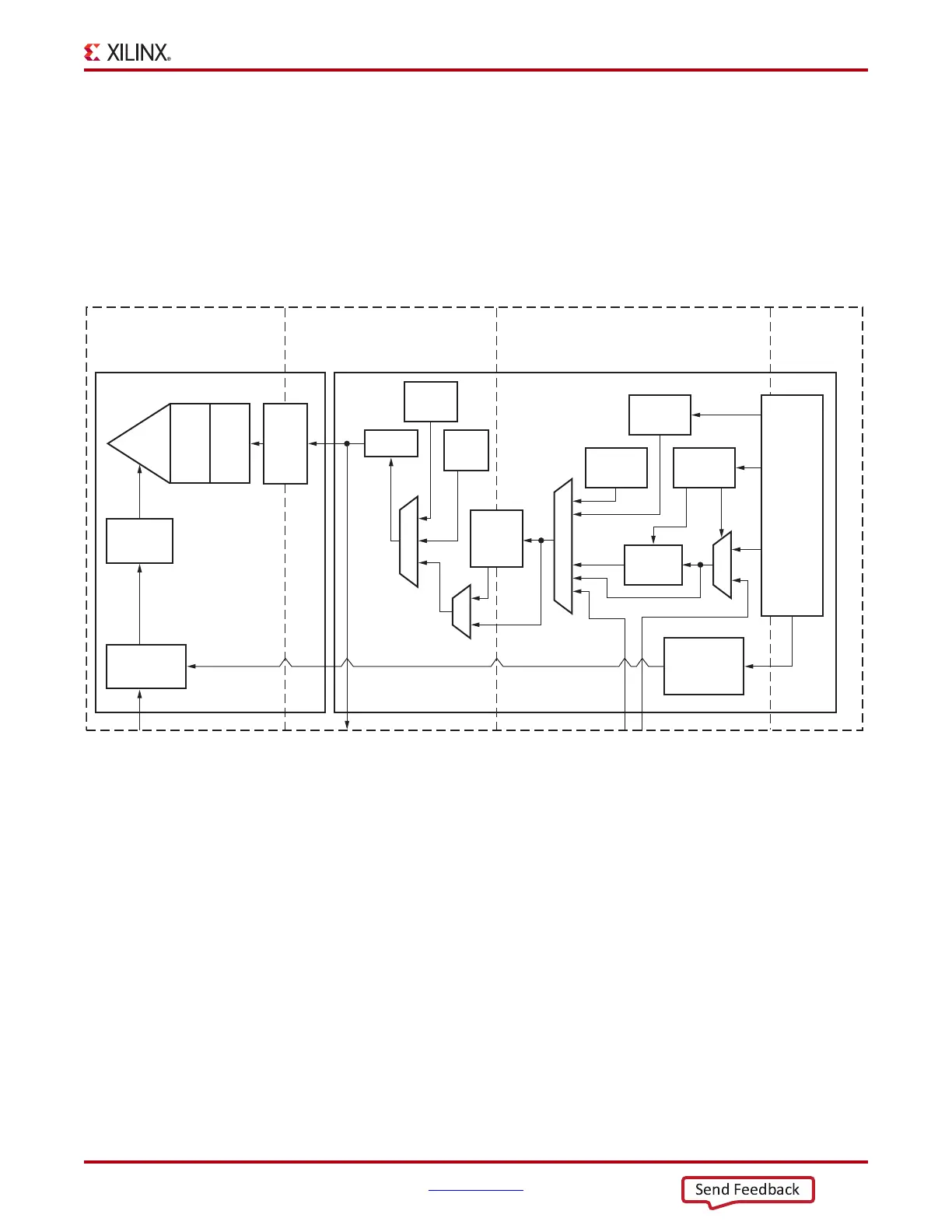
Functional Description
The GTP transceiver TX datapath has two internal parallel clock domains used in the PCS: the PMA
parallel clock domain (XCLK) and the TXUSRCLK domain. To transmit data, the XCLK rate must
match the TXUSRCLK rate, and all phase differences between the two domains must be resolved.
Figure 3-11 shows the XCLK and TXUSRCLK domains.
The GTP transceiver transmitter includes a TX buffer and a TX phase alignment circuit to resolve
phase differences between the XCLK and TXUSRCLK domains. The TX phase alignment circuit is
used when TX buffer is bypassed (see TX Pattern Generator, page 103). All TX datapaths must use
either the TX buffer or the TX phase alignment circuit. Table 3-12 shows trade-offs between
buffering and phase alignment.
X-Ref Target - Figure 3-11
Figure 3-11: TX Clock Domains
TX PMA
TX Serial Clock PMA Parallel Clock (XCLK) PCS Parallel Clock (TXUSRCLK)
FPGA Parallel
Clock
(TXUSRCLK2)
TX PCS
FPGA
TX
Interface
TX
Gearbox
UG482_C3_14_112811
TX PIPE
Control
Phase
Adjust
FIFO
PCIe
Beacon
From RX Parallel Data
(Far-End PMA Loopback)
To RX Parallel Data
(Near-End PCS Loopback)
Clock from PLL0 or PLL1
From RX Parallel Data
(Far-End PCS Loopback)
PISO
TX
Pre/
Post
Emp
TX Clock
Dividers
TX Phase
Interpolator
TX Phase
Interpolator
Controller
TX
OOB
and
PCIe
TX
Driver
Polarity
SATA
OOB
8B/10B
Encoder
Pattern
Generator