EasyManua.ls Logo

Xilinx Virtex UltraScale+ FPGAs User Manual

Xilinx Virtex UltraScale+ FPGAs
145 pages
To Next Page IconTo Next Page
To Previous Page IconTo Previous Page
Page #11 background imageLoading...
Page #11 background image
Implementation
It is a common pracce to dene the locaon of GTM transceiver Duals early in the design
process to ensure correct usage of clock resources and to facilitate signal integrity analysis during
board design. The implementaon ow facilitates this pracce through the use of locaon
constraints in the XDC le.
The posion of each GTM transceiver Dual primive is specied by an XY coordinate system that
describes the column number and the relave posion within that column. For a given device/
package combinaon, the transceiver with the coordinates X0Y0 is located at the lowest posion
of the lowest available bank.
There are two ways to create an XDC le for designs that ulize the GTM transceivers. The
preferred method is to use the UltraScale+ FPGAs GTM Transceivers Wizard. The Wizard
automacally generates XDC le templates that congure the transceivers and contain
placeholders for GTM transceiver placement informaon. The XDC les generated by the Wizard
can then be edited to customize operang parameters and placement informaon for the
applicaon.
The second approach is to create the XDC le manually. When using this approach, you must
enter both conguraon aributes that control transceiver operaon as well as the locaon
parameters. Care must be taken to ensure that all of the parameters needed to congure the
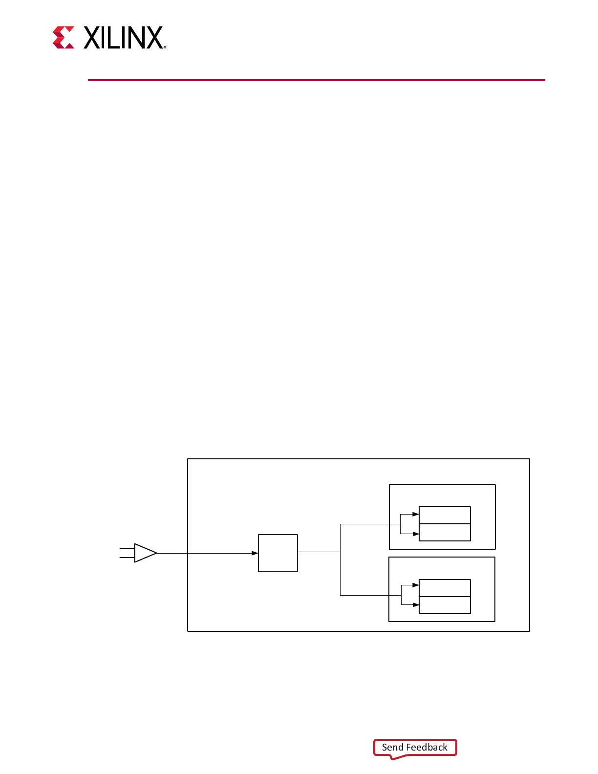
GTM transceiver are correctly entered. A GTM_DUAL primive must be instanated as shown in
the following gure.
Figure 3: One-Dual, Two-Channel Configuration (Reference Clock from the LCPLL)
LCPLL
GTM_DUAL
GTM Channel 0 (CH0)
RX
TX
GTM Channel 1 (CH1)
RX
TX
IBUFDS_GTM
X20212-061418
Each dual contains an LCPLL. Therefore, a reference clock can be connected directly to a
GTM_DUAL primive.
Chapter 1: Transceiver and Tool Overview
UG581 (v1.0) January 4, 2019 www.xilinx.com
Virtex UltraScale+ GTM Transceivers 11
Send Feedback
Question and Answer IconNeed help?

Do you have a question about the Xilinx Virtex UltraScale+ FPGAs and is the answer not in the manual?

Xilinx Virtex UltraScale+ FPGAs Specifications

General IconGeneral
BrandXilinx
ModelVirtex UltraScale+ FPGAs
CategoryTransceiver
LanguageEnglish

Summary

Chapter 1: Transceiver and Tool Overview

Features

Key features of the GTM transceiver, including supported line rates and modulation.

UltraScale+ FPGAs GTM Transceivers Wizard

Description of the wizard tool for configuring GTM transceivers.

Chapter 2: Shared Features

Reference Clock Selection and Distribution

Explanation of reference clock input options and selection architecture.

Reset and Initialization

Steps for initializing the GTM transceiver TX and RX datapaths.

Chapter 3: Transmitter

TX Interface

Gateway to the TX datapath, including data width and clocking.

TX FEC

Details on the Integrated KP4 Reed-Solomon Forward Error Correction.

TX Pattern Generator

Generates industry-standard PRBS patterns for signal integrity testing.

TX Configurable Driver

Controls output buffer characteristics like voltage and pre-emphasis.

Chapter 4: Receiver

RX Equalizer

Compensates for channel attenuation and distortion using CTLE, FFE, and DFE.

RX CDR

Clock Data Recovery circuit for extracting clock and data from incoming streams.

RX FEC

Details on the Integrated KP4 Reed-Solomon Forward Error Correction.

RX Interface

Gateway to the RX datapath, including data width and clocking.

Chapter 5: Board Design Guidelines

Related product manuals