Digital Monitor
The receiver uses an adapve algorithm in opmizing a link. The digital monitor provides visibility
into the current state of these adaptaon loops. Digital monitor requires a clock such as
DRPCLK. CH0/1_RXUSRCLK2 can be used for this. The aributes
CH0/1_RX_APT_CFG14A[15:12] and CH0/1_RX_APT_CFG18B[15:12] select the adaptaon
loops monitored on the CH0_DMONITOROUT and CH1_DMONITOROUT ports. The output
ports CH0_DMONITOROUT and CH1_DMONITOROUT contain the current code(s) for a
selected loop. A loop has three steady states: min, max, or dithering.
Ports and Attributes
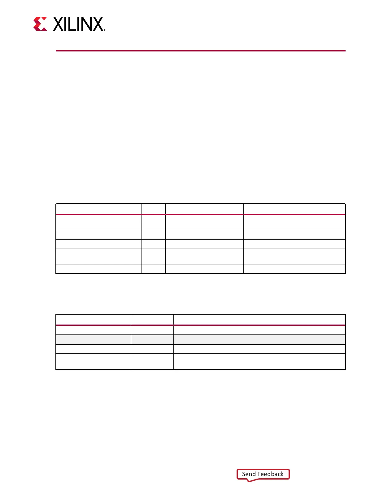
The following table shows the GTM digital monitor ports.
Table 26: Digital Monitor Ports
Port Dir Clock Domain Description
CH[0/1]_DMONITOROUT[31:0] Out Async/Local Clock Digital monitor output bus for channel
0/1.
CH[0/1]_DMONITORCLK In Async Channel 0/1 digital monitor clock.
CH[0/1]_DMONITORFIFORESET In Async Reserved. Tie to GND.
CH[0/1]_DMONITOROUTCLK Out Async Channel 0/1 internal clock from
adaptation loops.
DMONITOROUTPLLCLK Out Async Internal TX calibration clock.
The following table shows the GTM digital monitor aributes.
Table 27: Digital Monitor Attributes
Attribute Type Description
CH[0/1]_RX_MON_CFG 16-bit Reserved.
Bit Name Bit Field Description
DMON_ENABLE [0] Enables digital monitor for channel 0/1.
DMON_SRC [2:1] Enables RX DMON path for channel 0/1. Must be set to 2’b00 when
reading RX adaptation loops.
Chapter 2: Shared Features
UG581 (v1.0) January 4, 2019 www.xilinx.com
Virtex UltraScale+ GTM Transceivers 50
 Loading...

