Chapter 2
Shared Features
Reference Clock Input/Output Structure
The reference clock structure in the GTM transceiver supports two modes of operaon: input
mode and output mode. In the input mode of operaon, your design provides a clock on the
dedicated reference clock I/O pins that are used to drive the LCPLL. In the output mode of
operaon, the recovered clocks (RXRECCLK0 and RXRECCLK1) from any of the two channels
within the same Dual can be routed to the dedicated reference clock I/O pins. This output clock
can then be used as the reference clock input at a dierent locaon. The mode of operaon
cannot be changed during run me.
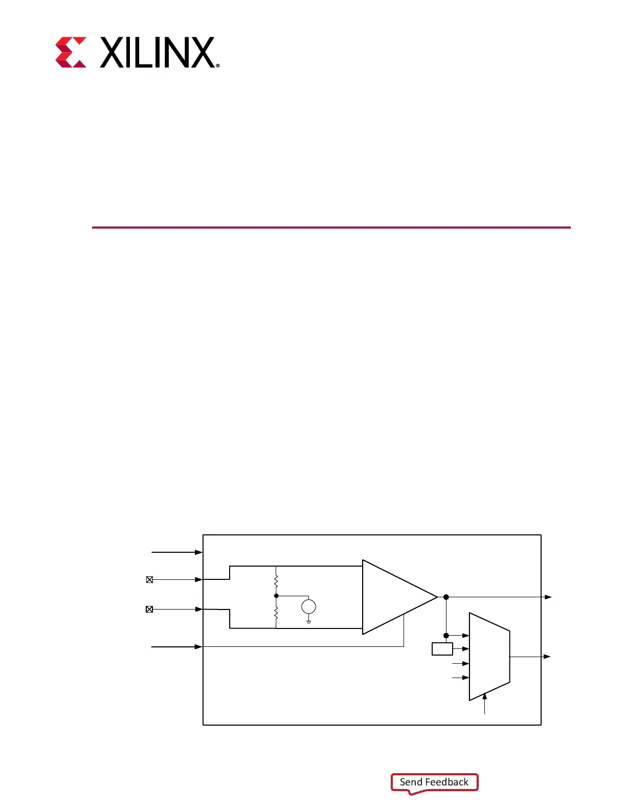
Input Mode
The reference clock input mode structure is illustrated in the following gure. The input is
terminated internally with 50Ω on each leg to MGTAVCC. The reference clock is instanated in
soware with the IBUFDS_GTM soware primive. The ports and aributes controlling the
reference clock input are ed to the IBUFDS_GTM soware primive.
Figure 4: Reference Clock Input Structure
2'b00
2'b01
2'b10
2'b11
IBUFDS_GTM
+
-
MGTAVCC
Nominal
50Ω
Nominal
50Ω
CEB
MGTAVCC
GTREFCLKN
GTREFCLKP
I
IB
/2
1'b0
Reserved
REFCLK_HROW_CK_SEL
To
HROW
To GTREFCLK or
GTM_DUAL
O
ODIV2
X20917-061418
Chapter 2: Shared Features
UG581 (v1.0) January 4, 2019 www.xilinx.com
Virtex UltraScale+ GTM Transceivers 12
 Loading...

