Each GTM transceiver features several loopback modes to facilitate tesng:
• Near-end PCS Loopback (Path 1 in the above gure). While in Near-end PCS Loopback, the RX
XCLK domain is clocked by the TX parallel clock (TX XCLK).
• Near-end PMA loopback (path 2 in the above gure).
• Far-end PCS Loopback (path 3 in the above gure). The transceiver in far-end PCS loopback
must use the same reference clock used by the transceiver that is the source of the loopbak
data.
Ports and Attributes
The following table denes the loopback ports.
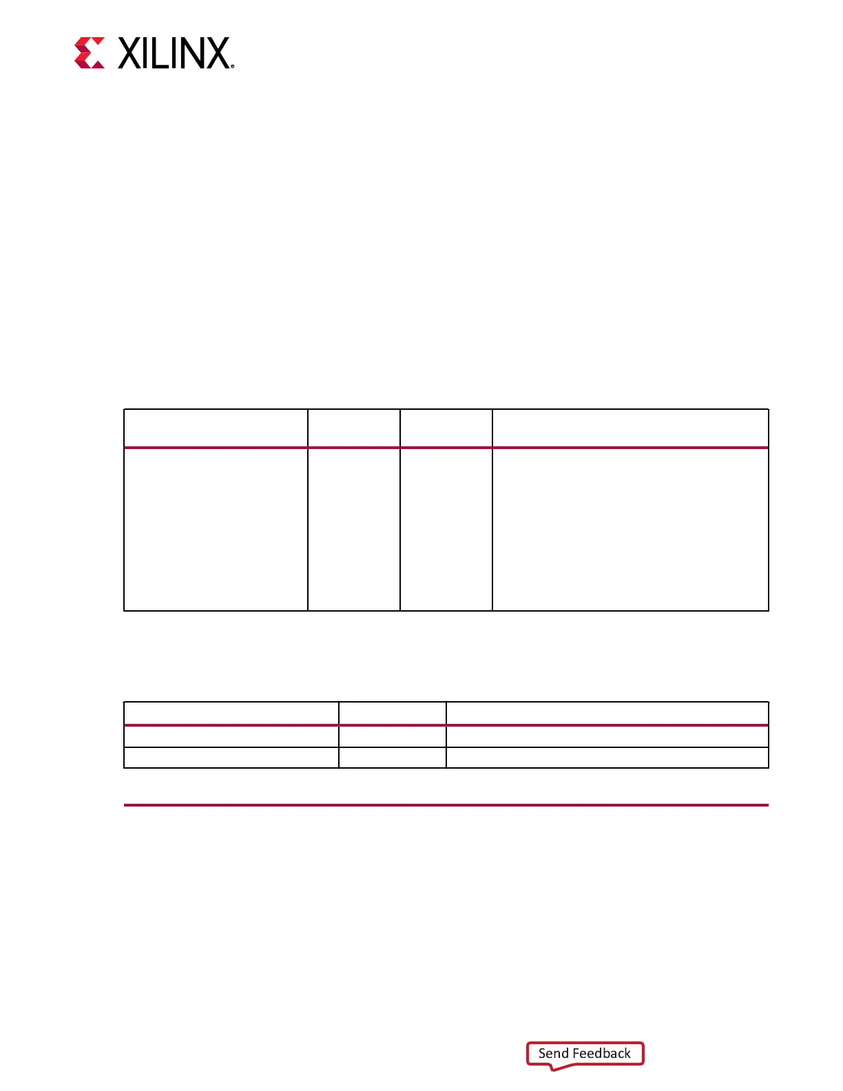
Table 23: Loopback Ports
Port Dir
Clock
Domain
Description
CH[0/1]_LOOPBACK[2:0] In Async Loopback control for channel 0/1:
3’b000: Normal operation.
3’b001: Near-End PCS Loopback.
3’b010: Near-End PMA Loopback.
3’b011: Reserved.
3’b100: Reserved.
3’b101: Reserved.
3’b110: Far-End PCS Loopback.
The following table denes the loopback aributes.
Table 24: Loopback Attributes
Attribute Type Description
CH[0/1]_TX_LPBK_CFG0 16-bit Reserved. Use the recommended value from the Wizard.
CH[0/1]_TX_LPBK_CFG1 16-bit Reserved. Use the recommended value from the Wizard.
Dynamic Reconfiguration Port
The dynamic reconguraon port (DRP) allows the dynamic change of parameters of the
GTM_DUAL primives. The DRP interface is a processor-friendly synchronous interface with an
address bus (DRPADDR) and separate data buses for reading (DRPDO) and wring (DRPDI)
conguraon data to the primives. An enable signal (DRPEN), a read/write signal (DRPWE), and
a ready/valid signal (DRPRDY) are the control signals that implement read and write operaons,
indicate operaon compleon, or indicate the availability of data.
Chapter 2: Shared Features
UG581 (v1.0) January 4, 2019 www.xilinx.com
Virtex UltraScale+ GTM Transceivers 47
 Loading...

